Display Device

Inactive Publication Date: 2010-03-04
PANASONIC LIQUID CRYSTAL DISPLAY CO LTD +1
View PDF8 Cites 40 Cited by
  • Summary
  • Abstract
  • Description
  • Claims
  • Application Information

AI Technical Summary

Benefits of technology

[0026]According to the display device of the present invention, the difference in intersecting-portion capacitance between the display region and the non-display region can be made small and hence, even when the route-around lines are used due to the formation of the window portion

Problems solved by technology

Accordingly, there arises a drawback that the drain line DL and the gate line GL which are separated exhibit an effective voltage different from an effective voltage of the drain line DL and the gate line GL which are not separated.
This drawback gives rise to a drawback that the in-plane effectiv

Method used


Image

  • Display Device
  • Display Device
  • Display Device

Examples


embodiment 1

Whole Constitution

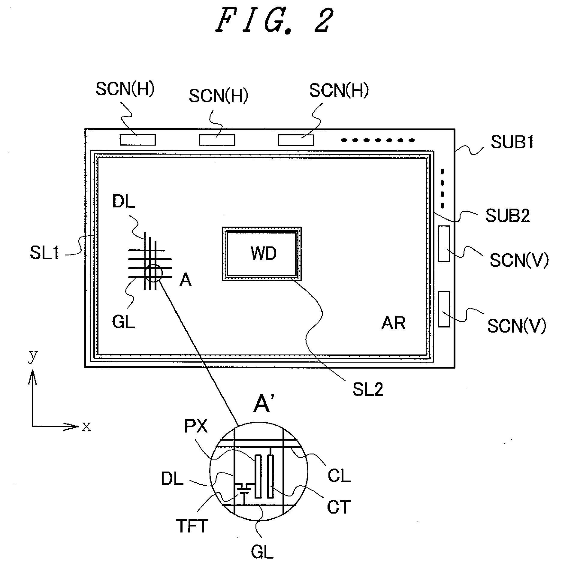
[0038]FIG. 2 shows a case in which a liquid crystal display device is taken as a display device to which the present invention is applied as an example, and FIG. 2 is also a view for explaining the schematic constitution of the liquid crystal display device according to the embodiment 1.

[0039]As can be clearly understood from FIG. 2, in a liquid crystal display device of an embodiment 1, a window portion (non-display region) WD constituted of an opening (through hole) is formed in a portion of a liquid crystal display region AR which is formed of amass of pixels. Due to such a constitution, for example, a user can observe a back-surface-side of the display device with his / her naked eyes.

[0040]Further, the liquid crystal display device of the embodiment 1 is constituted of a first substrate SUB1 on which pixel electrodes and the like are formed, a second substrate SUB2 which is arranged to face the first substrate SUB1 in an opposed manner, and a liquid crystal laye...

embodiment 2

[0090]FIG. 4A and FIG. 4B are views for explaining the schematic constitution of the liquid crystal display device of an embodiment 2 which constitutes the display device to which the present invention is applied, and FIG. 5A and FIG. 5B are enlarged views of an portion A in FIG. 4A. Here, FIG. 4A is a plan view of the liquid crystal display device of the embodiment 2 in which only drain lines DL, gate lines GL, drain route-around line JDL, and gate route-around line JGL are depicted, and FIG. 4B is a view for explaining one example of intersecting portions of drain route-around lines JDL and a gate route-around line JGL. Here, in FIG. 4B, FIG. 5A and FIG. 5B, an amorphous silicon layer AS′ is also shown.

[0091]The liquid crystal display device shown in FIG. 4A and FIG. 4B has the same constitution as the liquid crystal display device of the embodiment 1 except for the constitution of the drain route-around lines JDL and the gate route-around lines JGL which are formed in a periphera...

embodiment 3

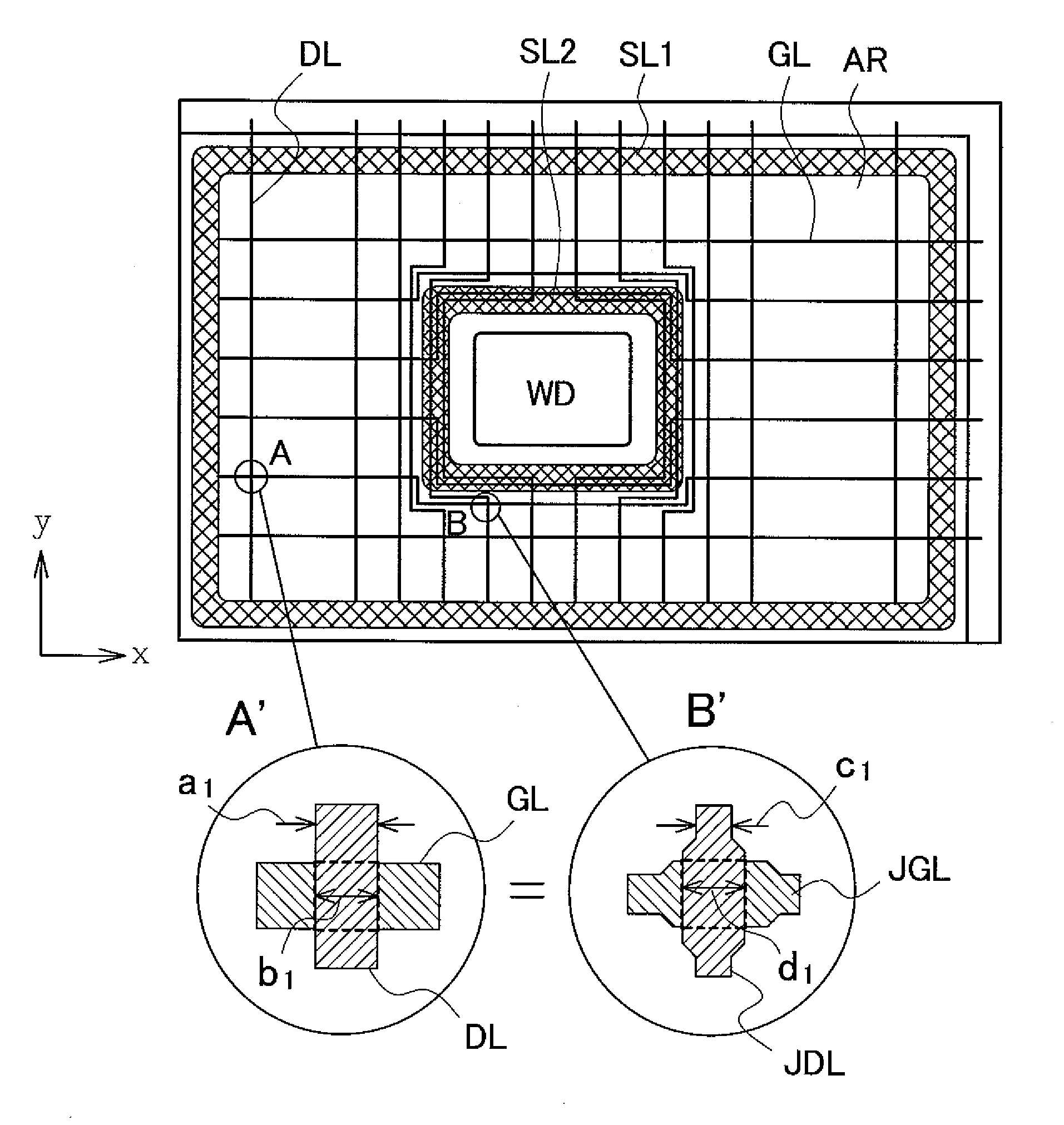
[0118]FIG. 6 is a view for explaining the schematic constitution of a liquid crystal display device of an embodiment 3 which is a display device to which the present invention is applied. FIG. 6 is also a view for explaining the schematic constitution of a region surrounded by a first sealing material SL1 and a second sealing material 2 in the liquid crystal display device of the embodiment 3.

[0119]In the liquid crystal display device of the embodiment 3, at an intersecting portion of a drain line DL and a gate line GL formed within a display region AR, as shown in an enlarged view A′ showing a portion indicated by a circle A in FIG. 6, respective line widths of the drain line DL and the gate line GL at the intersecting portion are set smaller than line widths of the respective lines DL, GL at portions other than the intersecting portion. In the embodiment 3, both line widths of the drain line DL and the gate line GL in an intersecting region are set smaller than the line widths of ...


PUM


Abstract

A display device in which a non-display region where drain lines, gate lines and pixels are not formed is formed at a portion within a display region which is constituted of a mass of the pixels, drain route-around lines and gate route-around lines are formed by routing the drain lines and the gate lines separated by the non-display region around the non-display region, a line width of at least one of the drain route-around line and the gate route-around line is set such that the line width at an intersecting portion where the drain route-around line and the gate route-around line intersect with each other differs from the line width at a non-intersecting portion.

Description

[0001]The present application claims priority from Japanese application JP2008-220624 filed on Aug. 29, 2008, the content of which is hereby incorporated by reference into this application.BACKGROUND OF THE INVENTION[0002]1. Field of the Invention[0003]The present invention relates to a display device, and more particularly, for example, to an active-matrix-type display device which includes a non-display region such as a window portion in a display portion.[0004]2. Description of the Related Art[0005]As shown in FIG. 8A, for example, an active-matrix-type display device is configured such that, a plurality of gate lines GL which extends in the x direction and is arranged parallel to each other in the y direction, and a plurality of drain lines DL which extends in the y direction and is arranged parallel to each other in the x direction, and in respective regions surrounded by these gate lines GL and drain lines DL, a pixel which is constituted of at least a thin film transistor whi...

Claims


Application Information

Patent Timeline
IPC IPC(8): G09G3/36
CPCG09G3/36G09G2320/0233G09G2320/0219G09G2300/0426
Inventor NAGASHIMA, OSAMUISHIGE, NOBUYUKISAKURAI, YASUSHI
Owner PANASONIC LIQUID CRYSTAL DISPLAY CO LTD
Why Eureka
Try Eureka