Optical Condition Design Method for a Compound-Eye Imaging Device

a technology of optical condition and imaging device, which is applied in the field of optical condition design method of compound eye imaging device, can solve the problems of not being able to always stably not being able to increase the definition of the reconstructed image, so as to achieve stably obtain the reconstructed, reduce the portion of the same image information, and high definition

Inactive Publication Date: 2010-03-04
FUNAI ELECTRIC CO LTD +1
View PDF5 Cites 191 Cited by
  • Summary
  • Abstract
  • Description
  • Claims
  • Application Information

AI Technical Summary

Benefits of technology

[0013]An object of the present invention is to provide an optical condition design method for a compound-eye imaging device which makes it possible to reduce portions of the same image information in multiple unit images captured in the compound-eye imaging device, and to stably obtain a reconstructed image having a high definition.
[0015]The optical condition design method for a compound-eye imaging device according to the present invention determines the optical condition of the optical lenses to achieve a large dispersion of the pixel observation points on the at least one imaginary object planes. This makes it possible to stably reduce the number of pixels which image the same portions of the target object, making it possible to reduce portions of the same image information in the multiple unit images, and obtain a reconstructed image having a high definition.
[0016]Preferably, the at least one imaginary object plane set in the plane setting step is multiple imaginary object planes at different distances from the optical lenses, and the optimum optical condition determined in the condition determining step is a set of variables giving a maximum total dispersion in all the multiple imaginary object planes. This preferred mode of the present invention makes it possible to determine the optimum optical condition based on the dispersion of the pixel observation points on multiple imaginary object planes, so that it is possible to more surely reduce the number of pixels which image the same portions of the target object.
[0017]Further preferably, the multiple imaginary object planes set in the plane setting step include a plane at an essentially infinite distance from the optical lenses, and a plane at a distance D from the optical lenses which satisfies the following equation:D=Ld·B / Gd·k where Ld is average distance between the solid-state imaging element and the optical lenses, B is average distance between adjacent optical lenses, Gd is average distance between adjacent pixels, and k is an integer of at least one. This makes it possible to evaluate the dispersion of the pixel observation points on the imaginary object planes where localizations of the pixel observation points are likely to occur. Thus, it is possible to more efficiently reduce the number of pixels which image the same portions of the target object.
[0018]Further preferably, the evaluating step calculates sum area of the unit surfaces containing at least one pixel observation point, and calculates ratio of the sum area to total area of the at least one imaginary object plane, and evaluates the dispersion of the pixel observation points by using the ratio of the sum area to the total area of the at least one imaginary object plane. This makes it possible to more efficiently evaluate the dispersion of the pixel observation points.
[0019]Still further preferably, the evaluating step calculates the number of pixel observation points of each unit surface as a local density of the each unit surface, and evaluates the dispersion of the pixel observation points using variance of the local densities of the unit surfaces. This makes it possible to more accurately evaluate the dispersion of the pixel observation points.

Problems solved by technology

However, depending on a random number used to determine the arrangement of the optical lenses, the random arrangement of optical lenses described above may incidentally cause the intersection points between the paths of lights h1, h2 .
In this case, it is not possible to increase the definition of the reconstructed image.
In short, the random arrangement of optical lenses does not make it possible to always stably increase the definition of the reconstructed image.

Method used


Image

  • Optical Condition Design Method for a Compound-Eye Imaging Device
  • Optical Condition Design Method for a Compound-Eye Imaging Device
  • Optical Condition Design Method for a Compound-Eye Imaging Device

Examples


first embodiment

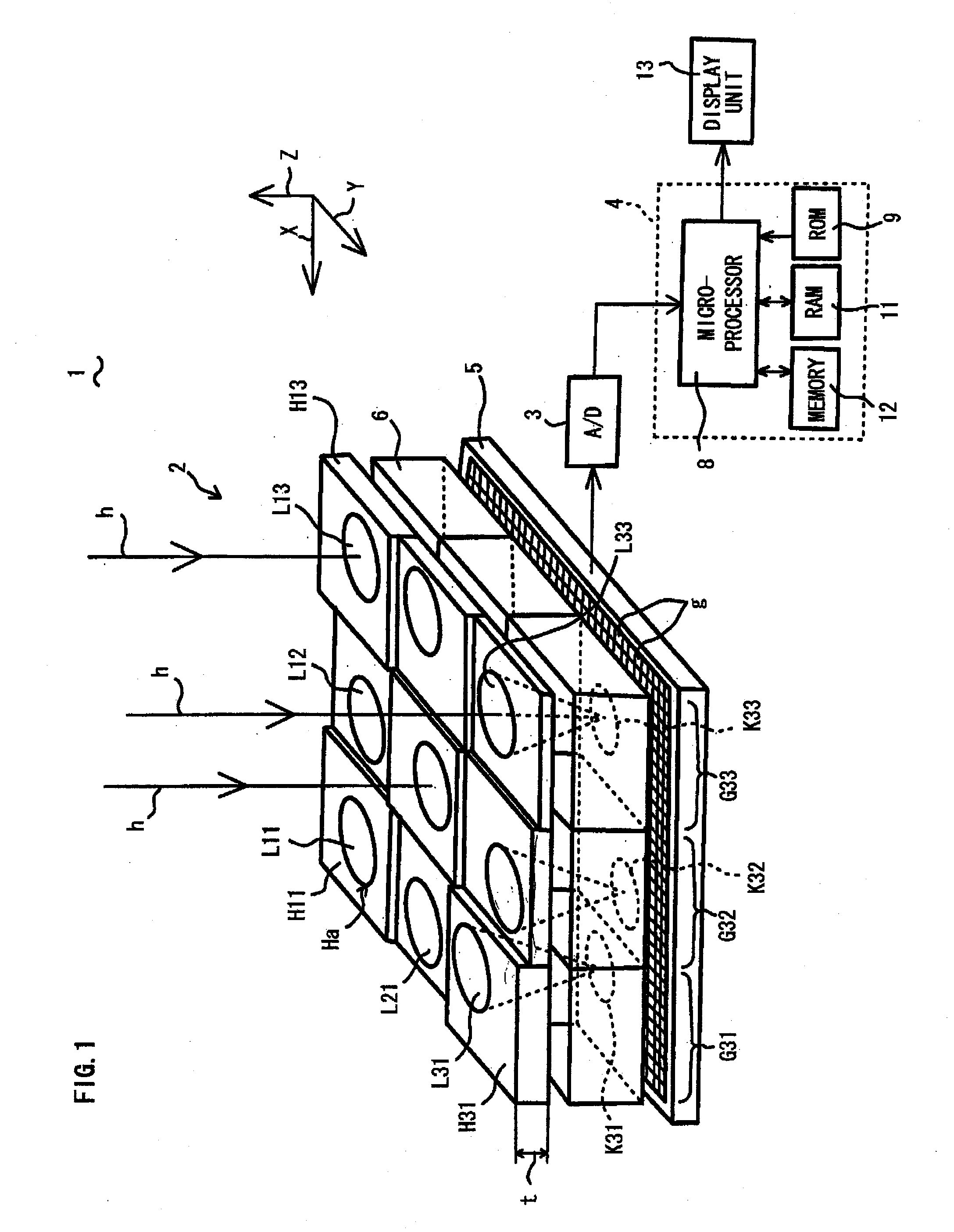
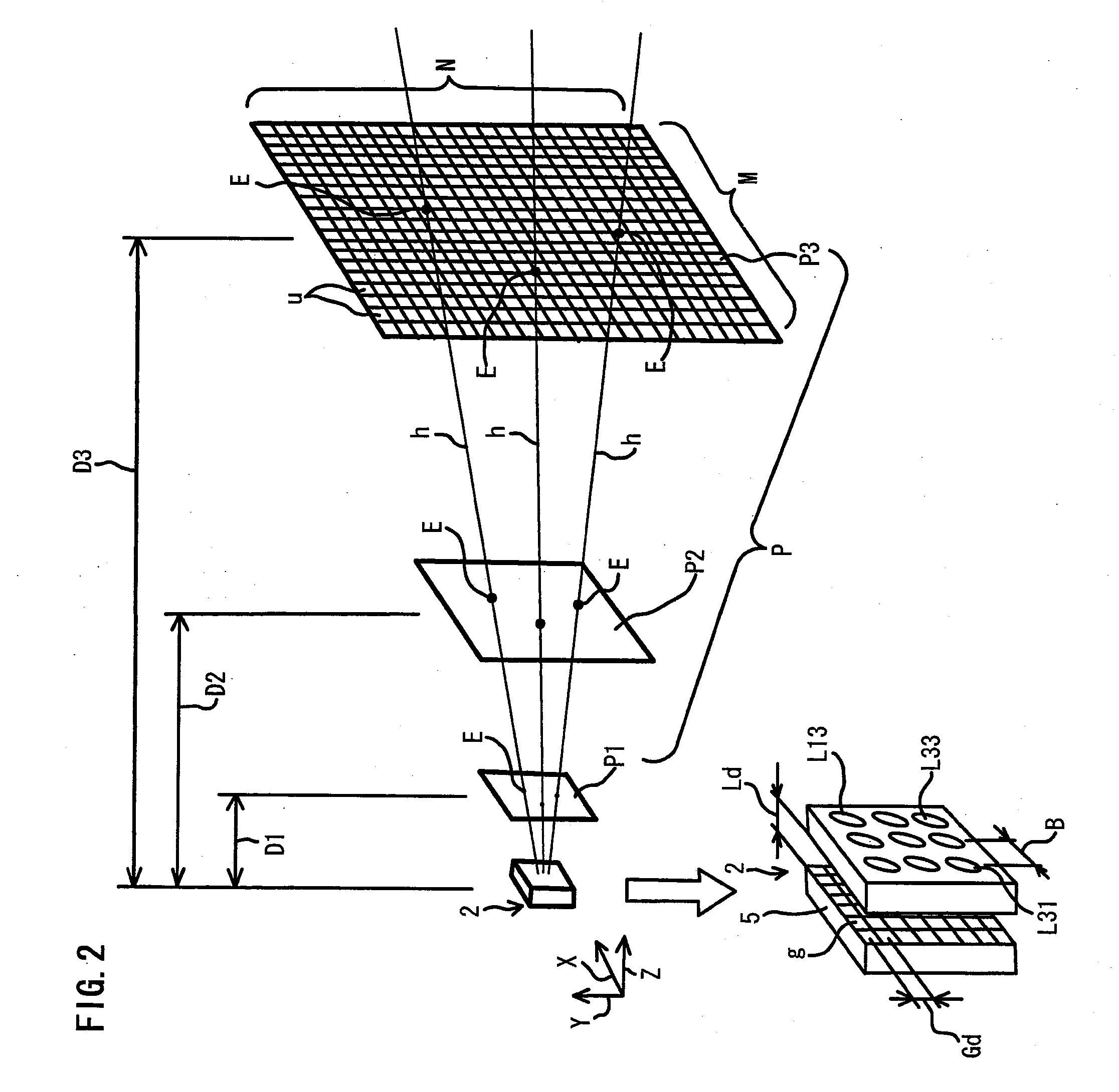
[0034]An optical condition design method for a compound-eye imaging device 1 according to a first embodiment of the present invention will be described with reference to FIG. 1 to FIG. 3. FIG. 1 is a schematic perspective view, with a block diagram, of the compound-eye imaging device 1 formed based on optical conditions determined by the optical condition design method according to the first embodiment. As shown in FIG. 1, the compound-eye imaging device 1 comprises an imaging device body 2 for collecting lights h from a target object and forming an image therefrom, and an image processing unit 4 connected to the imaging device body 2 via an AD (Analog-to-Digital) converter 3 for forming a reconstructed image from image information (multiple unit images) output from the imaging device body 2.

[0035]The imaging device body 2 comprises: 9 (nine) optical lenses L11, L12 . . . L33 for collecting lights h from the target object at different angles, respectively; holders H11, H12 . . . H33...

second embodiment

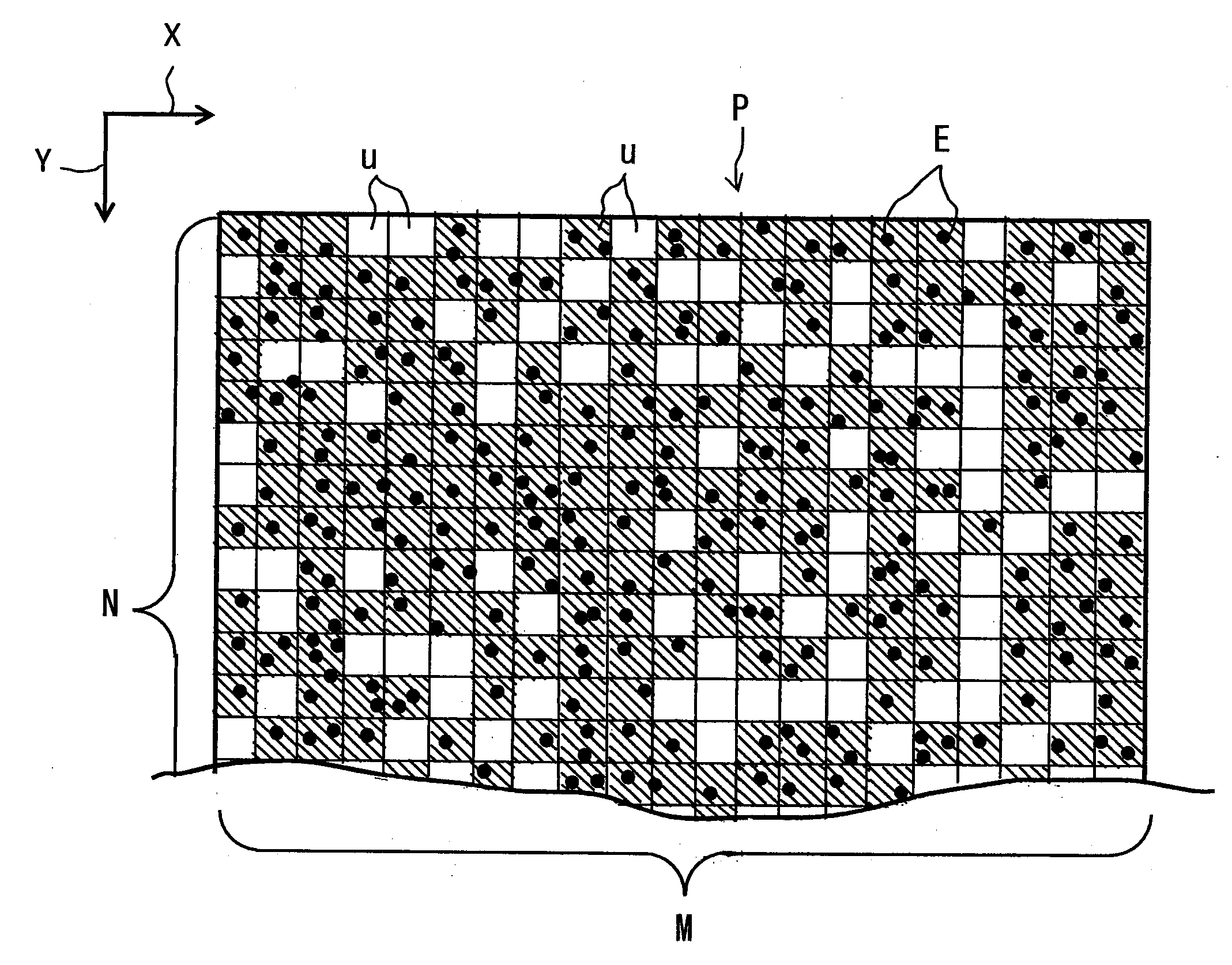
[0053]Referring to FIG. 4, an optical condition design method according to a second embodiment of the present invention will be described. FIG. 4 is a schematic enlarged view showing an imaginary object (target object) plane used in the present embodiment. The present embodiment is basically the same as the first embodiment except for the evaluating step and the condition determining step. In the first embodiment, the ratio of the unit surfaces u having at least one pixel observation point E is calculated using the coverage ratio R so as to determine that a higher coverage ratio R corresponds to a larger dispersion of the pixel observation points E. On the other hand, in the evaluating step of the present embodiment, the number of pixel observation points E of each unit surface u is calculated as a local density of the each unit surface u, and the variance (meaning the same as variance in the statistics) of the local densities of the unit surfaces u is evaluated as a dispersion of t...

example

[0058]An example of the present invention and comparative examples were prepared and compared as follows. The three-dimensional position of the optical lenses L11, L12 . . . L33 were set as variables, and the downhill simplex method was used as an algorithm to change each variable each time to allow sufficient number of successive changes of the variables so as to obtain values of the variables giving a maximum total coverage ratio R (optimum optical condition). Four imaginary object planes P were set at distances of 0.2 m (meter), 0.4 m, 5 m and 10 m, respectively, from the compound-eye imaging device 1. The number of unit surfaces u on each of the imaginary object planes P was set to be the same as the number of the pixels g of the solid-state imaging element 5. More specifically, the numbers M and N of unit surfaces u in the X and Y directions of each imaginary object plane P were set to be the same as the numbers of pixels g in the X and Y directions of the solid-state imaging e...


PUM


Abstract

An imaginary object plane is set in front of an imaging device body (plane setting step). A part of optical conditions of optical lenses are changed as variables, and positions of points (pixel observation points) on the imaginary object plane where lights coming from pixels of a solid-state imaging element and back-projected through the optical lenses are calculated (pixel observation point calculating step). The dispersion in position of the calculated pixel observation points is evaluated (evaluating step). Finally, a set of values of the variables giving maximum evaluated dispersion of the calculated pixel observation points is determined as optimum optical condition of the optical lenses (condition determining step). This reduces the number of pixels which image the same portions of the target object, making it possible to reduce portions of the same image information in multiple unit images, and to stably obtain a reconstructed image having a high definition.

Description

BACKGROUND OF THE INVENTION[0001]1. Field of the Invention[0002]The present invention relates to an optical condition design method for a compound-eye imaging device.[0003]2. Description of the Related Art[0004]A compound-eye imaging device is known which comprises an optical lens array having multiple micro optical lenses, and a solid-state imaging element (photodetector array) for imaging multiple unit images of a target object which are formed by the respective optical lenses of the optical lens array so as to reconstruct the multiple unit images into a high definition reconstructed image (refer to e.g. Japanese Laid-open Patent Publication 2001-61109). FIG. 8 is a schematic perspective view of such a conventional compound-eye imaging device 100.[0005]As shown in FIG. 8, the compound-eye imaging device 100 has an optical lens array 101 having micro optical lenses L11, L12 . . . L33 equidistantly arranged in a matrix of rows and columns, and a solid-state imaging element 102 for i...

Claims


Application Information

Patent Timeline
Patent Type & Authority Applications(United States)
IPC IPC(8): G01B9/00
CPCH01L27/14625H01L27/14685H04N5/349H04N5/2259H04N5/2254H04N23/58H04N25/48
Inventor TANIDA, JUNHORISAKI, RYOICHINAKAO, YOSHIZUMITOYODA, TAKASHIMASAKI, YASUO
Owner FUNAI ELECTRIC CO LTD
Why Eureka
Try Eureka