Semiconductor device and internal combustion engine ignition device

a technology of semiconductor elements and ignition devices, which is applied in the direction of ignition safety means, machines/engines, pulse techniques, etc., can solve the problems of difficult to keep balance in the control circuit, the size of the semiconductor element cannot be reduced, and the achievement of low resistance cannot lead to cost reduction, etc., to achieve small control circuits, simple control circuits, and elimination of feedback loops

Inactive Publication Date: 2010-03-11
FUJI ELECTRIC CO LTD
View PDF6 Cites 40 Cited by
  • Summary
  • Abstract
  • Description
  • Claims
  • Application Information

AI Technical Summary

Benefits of technology

[0029]According to the invention, the IGBT having the saturation current value in the limiting current value range of the semiconductor device is used in place of a current limiting circuit using a sense IGBT, so that a feedback loop can be eliminated. In addition, the use of saturation characteristic of the IGBT brings the current flowing in the IGBT to a current limiting state naturally without exceeding the saturation current value of the IGBT. Accordingly, current overshoot does not occur, so that vibration of the waveform of the current flowing in the IGBT can be suppressed. In this manner, a gate voltage can be kept constant. In addition, since a current limiting circuit requiring a complicated structure is not used, a control circuit can be made small-sized and simple. Thus, the total size of the semiconductor device can be reduced to attain cost reduction.
[0030]According to the to the invention, there is an effect that vibration of the waveform of the current flowing in the IGBT can be suppressed to thereby keep a gate voltage constant. In addition, there is another effect that the total size of the semiconductor device can be reduced to attain cost reduction.

Problems solved by technology

Because the semiconductor device needs to have a predetermined volume in order to ensure the tolerance of the semiconductor device, it is impossible to make the size of the semiconductor element smaller than a certain predetermined size.
For this reason, achievement of low on-resistance cannot lead to cost reduction based on reduction of the size of the semiconductor device.
It is hence very difficult to keep balance in the control circuit.
In addition, since the current control circuit has a complicated structure and requires the sense IGBT, the control circuit is large-sized.
For this reason, there occurs a problem that the total size of the semiconductor device is large to result in cost increase.

Method used


Image

  • Semiconductor device and internal combustion engine ignition device
  • Semiconductor device and internal combustion engine ignition device
  • Semiconductor device and internal combustion engine ignition device

Examples


embodiment 1

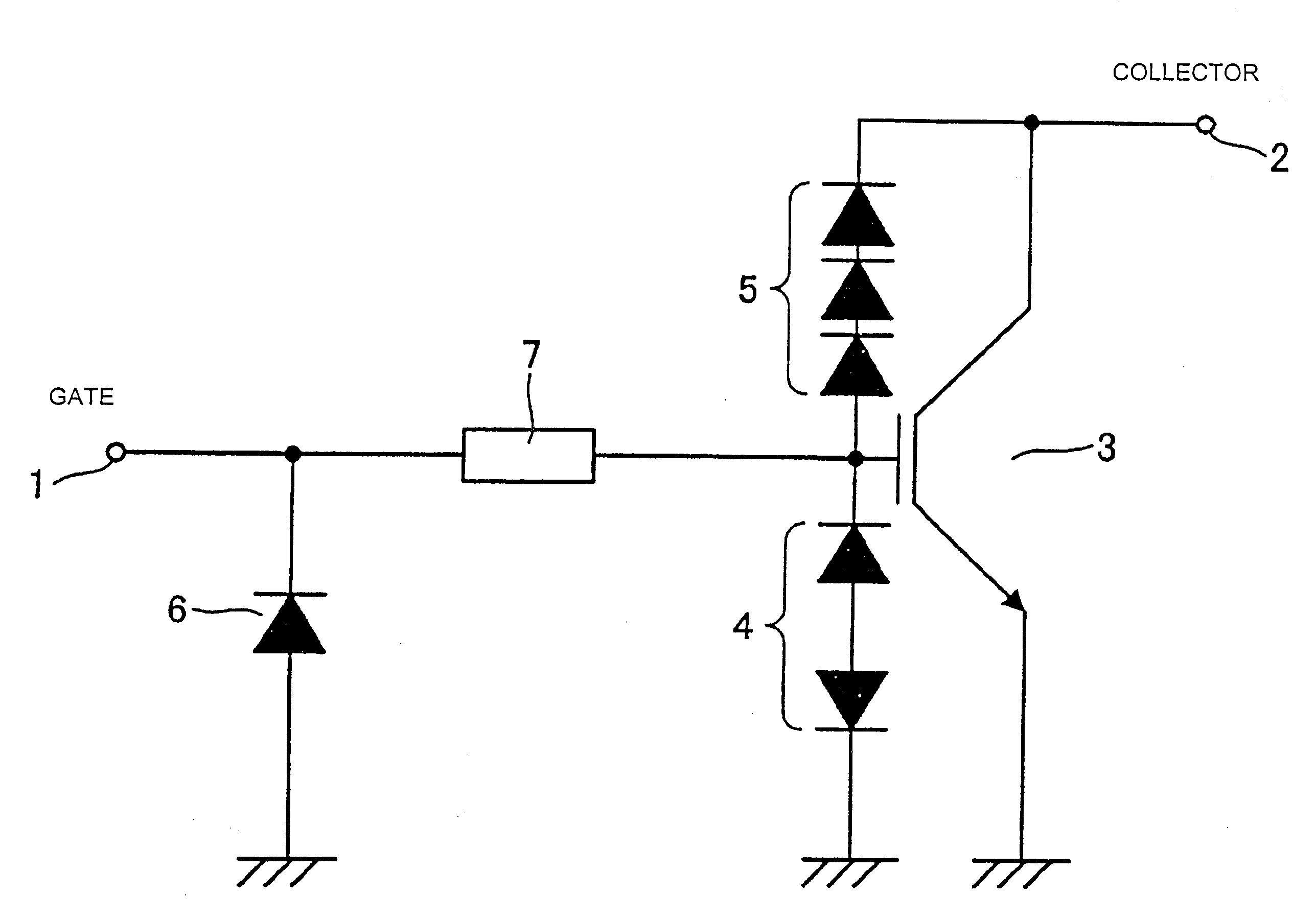
[0056]An emitter resistor may be provided between the emitter of the IGBT 3 and the ground. FIG. 3 is a circuit diagram showing another example of the semiconductor switch having the constant voltage circuit according to The semiconductor switch is additionally provided with an emitter resistor 8. When a saturation current flows into the IGBT 3, a practically effective gate voltage of the IGBT 3 decreases due to voltage drop of the emitter resistor 8 so that the saturation current of the IGBT 3 decreases. When a current in a normal operation range flows into the IGBT 3, the voltage drop of the emitter resistor 8 is small so that the influence of the emitter resistor 8 on an on-voltage becomes small. The reason will be described later.

[0057]Since a current flowing in the IGBT 3 decreases in accordance with temperature rise of the IGBT 3 in a saturation region, the constant voltage circuit 7 may be provided with a function of increasing the gate voltage in accordance with the tempera...

embodiment 4

[0071]As described above, since the IGBT 33 and the control circuit 32 are formed separately on different semiconductor substrates , the IGBT 33 and the control circuit 32 can be produced in the most suitable manufacturing processes respectively. Therefore, high-level control suitable for the IGBT 33 and the control circuit 32 can be performed.

embodiment 5

[0072]FIG. 8 is a sectional view showing a semiconductor device in which resistors are built in an IGBT. In Embodiment 5, emitter resistors are formed in a planar gate type IGBT. As shown in FIG. 8, similarly to the planar gate type IGBT (see FIG. 5) in


PUM


Abstract

A semiconductor device includes an IGBT, a constant voltage circuit, and protection Zener diodes. The IGBT makes/breaks a low-voltage current flowing in a primary coil. The constant voltage circuit and the protection Zener diodes are provided between an external gate terminal and an external collector terminal. The constant voltage circuit supplies a constant gate voltage to the IGBT to thereby set a saturation current value of the IGBT to a predetermined limiting current value. The IGBT has the saturation current value in a limiting current value range of the semiconductor device.

Description

BACKGROUND OF THE INVENTION[0001]The present invention relates to a semiconductor device. Particularly it relates to a current-limited semiconductor device connected to a load.[0002]An example of a current-limited semiconductor device is an internal combustion engine ignition device (igniter). The internal combustion engine ignition device is a device, for example, that is provided for controlling a gasoline engine used in a car or the like, which is provided with a spark plug for starting combustion by igniting an air-fuel mixture such as an air-gasoline mixture imported into a combustion chamber. FIG. 18 is a conceptual view showing an example of the internal combustion engine ignition device. As shown in FIG. 18, the internal combustion engine ignition device includes primary and secondary coils 201 and 202 provided as ignition coils, a switching unit 203 which turns on and off a low-voltage current flowing in the primary coil 201, a battery 204 which supplies electric power to t...

Claims


Application Information

Patent Timeline
Patent Type & Authority Applications(United States)
IPC IPC(8): F02P3/04H01L29/739
CPCF02P3/051F02P11/02H01L27/0623H01L27/0883H03K17/0828H01L29/0847H01L29/7395H03K17/08128H01L29/0696
Inventor UENO, KATSUNORI
Owner FUJI ELECTRIC CO LTD
Why Eureka
Try Eureka