

Printed circuit board and manufacturing method
a technology of printed circuit boards and manufacturing methods, applied in the direction of dielectric characteristics, thermoplastic polymer dielectrics, electric/magnetic/electromagnetic heating, etc., can solve the problem of difficult to provide sufficient adhesion between the insulating layer and the conductive pattern
- Summary
- Abstract
- Description
- Claims
- Application Information
AI Technical Summary
Benefits of technology
Problems solved by technology
Method used
Image

Examples
experiment 1
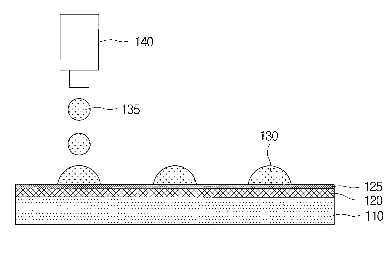
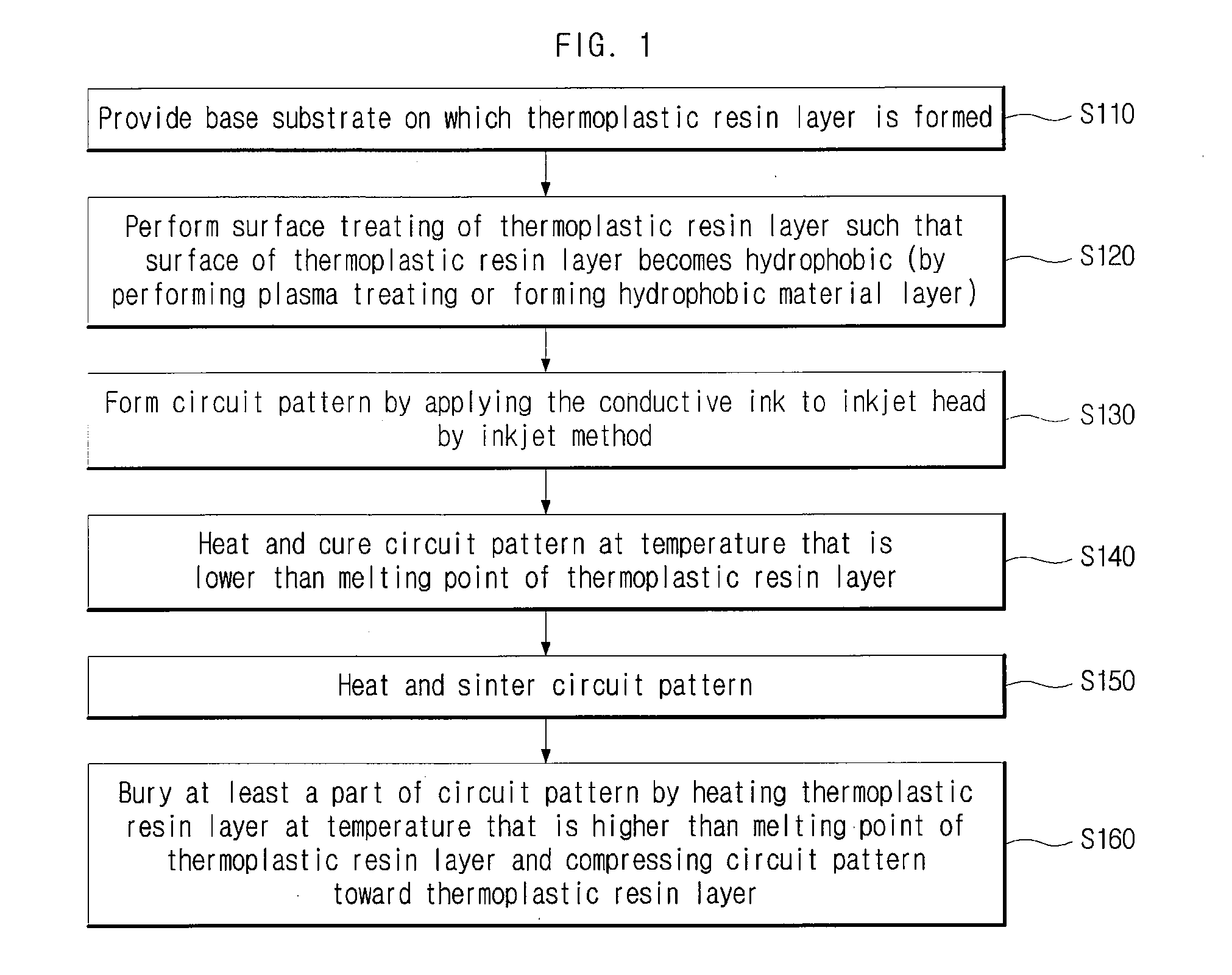
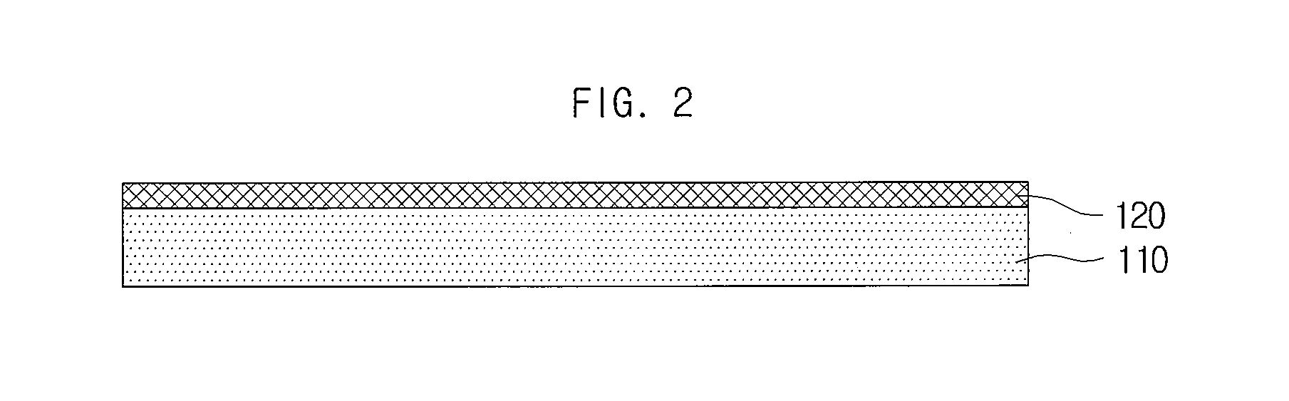
[0056]The thermoplastic resin layer 120 made of polyvinyl butyral is coated on the base substrate 110 made of bismaleimide triazine resin. Then, the circuit pattern 130 is formed by an inkjet method and is cured and sintered at the temperature of 200° C. in the reducing atmosphere. Thereafter, a part of the circuit pattern 130′ is buried in the thermoplastic resin layer 120 at the temperature of 200° C. and under the pressure of 20 MPa.
[0057]The bonding strength between the circuit pattern 130′ and the thermoplastic resin layer 120 in the printed circuit board manufactured by the aforementioned operations is tested to have been increased to 1.1 N / mm. For the reference, in the case of using no thermoplastic resin layer 120 and the circuit pattern 130′ that is not buried, the bonding strength was 0.11 N / mm.
[0058]Next, a printed circuit board will be described according to an embodiment based on another aspect of the present invention
[0059]FIG. 8 is a cross-sectional view showing a pri...
PUM
| Property | Measurement | Unit |
|---|---|---|
| Temperature | aaaaa | aaaaa |
| Force | aaaaa | aaaaa |
| Melting point | aaaaa | aaaaa |
Abstract
Description
Claims
Application Information