
Semiconductor transistor device with improved isolation arrangement, and related fabrication methods

a technology of isolation arrangement and semiconductor, applied in the direction of semiconductor devices, basic electric elements, electrical equipment, etc., can solve the problems of significant yield reduction, unfavorable aspect ratio of gap filling process, and loss of sti oxide, so as to inhibit sti oxide loss and reduce or eliminate the loss of sti material

Inactive Publication Date: 2010-03-11
ADVANCED MICRO DEVICES INC
View PDF5 Cites 0 Cited by
  • Summary
  • Abstract
  • Description
  • Claims
  • Application Information

AI Technical Summary

Benefits of technology

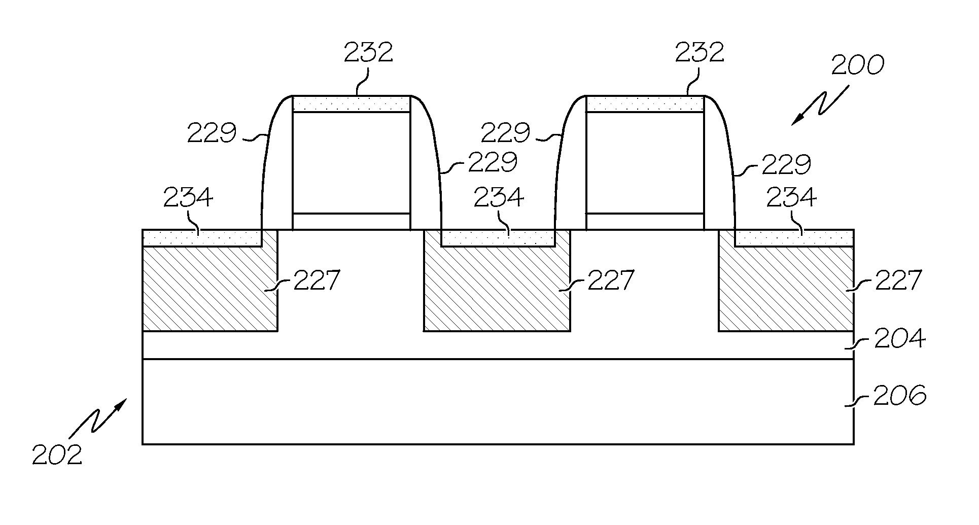
[0006]The techniques and technologies described herein can be utilized to reduce or eliminate the loss of STI material during the fabrication of a MOS transistor device. A MOS transistor device fabricated in accordance with the process described herein employs a buried nitride layer within the STI region, and the buried nitride region is effective at inhibiting STI oxide loss during certain process steps, such as silicidation steps.

Problems solved by technology

With the introduction of new semiconductor device fabrication processes and materials (such as eSiGe, eSiC, high-k material, etc.), loss of the STI oxide is becoming problematic.
Increased STI oxide loss, along with shrinking device pitch, creates an unfavorable aspect ratio for gap fill processes.
This can result in significant yield reductions, particularly for small process technology nodes (for example, 45 nm technology).
Problems associated with the loss of STI material might worsen as process technologies continue to develop and with the integration of newer materials.
However, this involves significant process development and such methods may not adequately inhibit the loss of STI material.
Moreover, most of the STI loss occurs during formation of silicide elements because conventional silicidation processes use significant amounts of hydrofluoric acid based (HF) wet etches.

Method used


Image

  • Semiconductor transistor device with improved isolation arrangement, and related fabrication methods
  • Semiconductor transistor device with improved isolation arrangement, and related fabrication methods
  • Semiconductor transistor device with improved isolation arrangement, and related fabrication methods

Examples


Embodiment Construction

[0014]The following detailed description is merely illustrative in nature and is not intended to limit the embodiments of the subject matter or the application and uses of such embodiments. As used herein, the word “exemplary” means “serving as an example, instance, or illustration.” Any implementation described herein as exemplary is not necessarily to be construed as preferred or advantageous over other implementations. Furthermore, there is no intention to be bound by any expressed or implied theory presented in the preceding technical field, background, brief summary or the following detailed description.

[0015]For the sake of brevity, conventional techniques related to semiconductor device fabrication may not be described in detail herein. Moreover, the various tasks and process steps described herein may be incorporated into a more comprehensive procedure or process having additional steps or functionality not described in detail herein. In particular, various steps in the manu...


PUM


Abstract

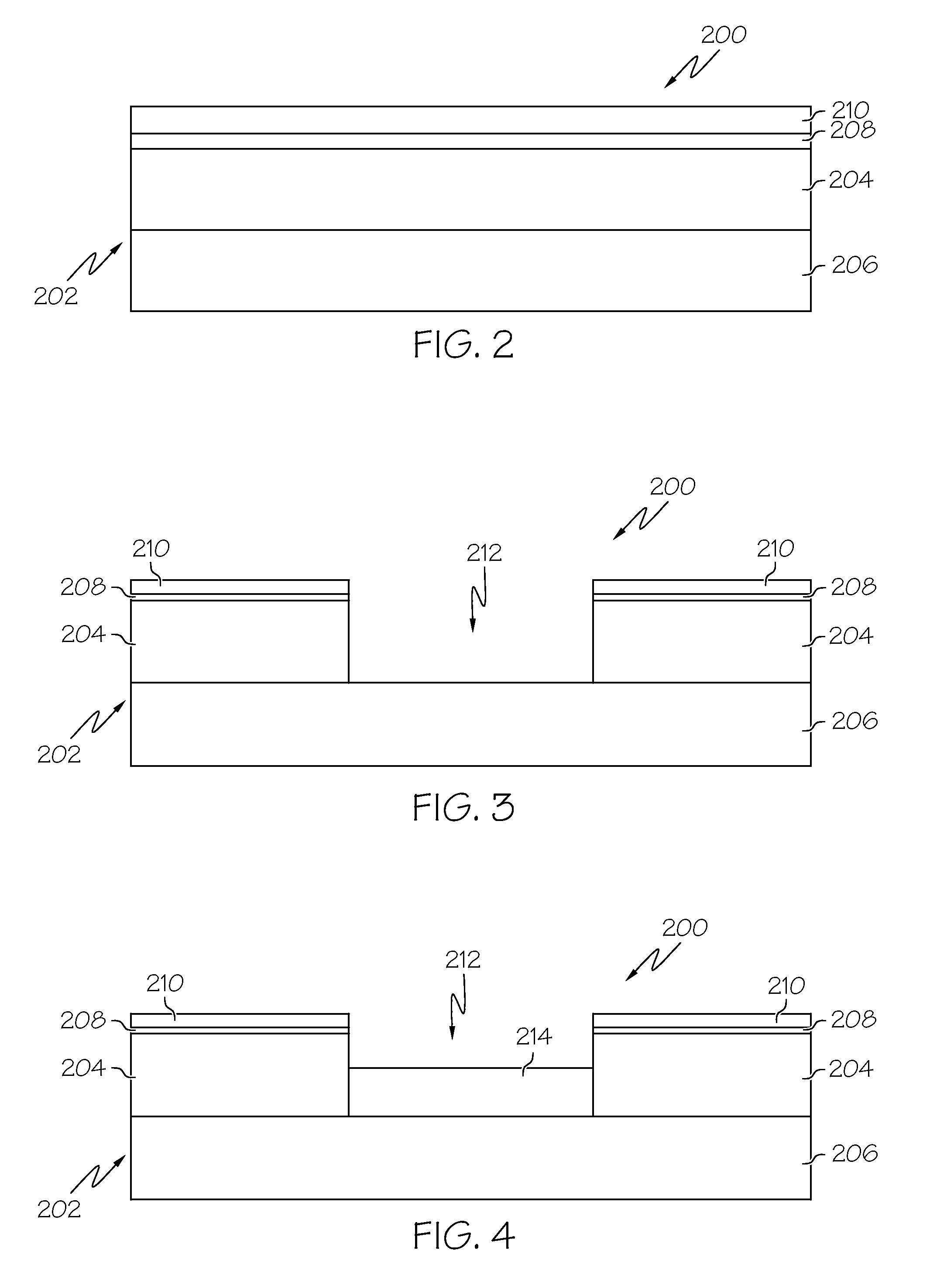
A method of fabricating a semiconductor device structure is provided. The method begins by providing a substrate having a layer of semiconductor material, a pad oxide layer overlying the layer of semiconductor material, and a pad nitride layer overlying the pad oxide layer. The method proceeds by selectively removing a portion of the pad nitride layer, a portion of the pad oxide layer, and a portion of the layer of semiconductor material to form an isolation trench. Then, the isolation trench is filled with a lower layer of isolation material, a layer of etch stop material, and an upper layer of isolation material, such that the layer of etch stop material is located between the lower layer of isolation material and the upper layer of isolation material. The layer of etch stop material protects the underlying isolation material during subsequent fabrication steps.

Description

TECHNICAL FIELD[0001]Embodiments of the subject matter described herein relate generally to semiconductor devices. More particularly, embodiments of the subject matter relate to the use of isolation regions between metal oxide semiconductor transistors.BACKGROUND[0002]The majority of present day integrated circuits (ICs) are implemented by using a plurality of interconnected field effect transistors (FETs), which may be realized as metal oxide semiconductor field effect transistors (MOSFETs or MOS transistors). A MOS transistor may be realized as a p-type device (i.e., a PMOS transistor) or an n-type device (i.e., an NMOS transistor). Moreover, a semiconductor device can include both PMOS and NMOS transistors, and such a device is commonly referred to as a complementary MOS or CMOS device. A MOS transistor includes a gate electrode as a control electrode that is formed over a semiconductor substrate, and spaced-apart source and drain regions formed within the semiconductor substrate...

Claims


Application Information

Patent Timeline
Patent Type & Authority Applications(United States)
IPC IPC(8): H01L29/00H01L21/76
CPCH01L21/823412H01L21/823425H01L21/823481H01L29/7848H01L21/823878H01L29/665H01L21/823807
Inventor PAL, ROHITBROWN, DAVIDLUNING, SCOTT
Owner ADVANCED MICRO DEVICES INC
Learn More