Method of etching sacrificial layer, method of manufacturing MEMS device, MEMS device and MEMS sensor

a technology of etching sacrificial layer and manufacturing method, which is applied in the direction of semiconductor electrostatic transducers, semiconductor device details, electrical transducers, etc., can solve the disadvantageous complexity of manufacturing steps of silicon microphones b>101/b>, suppress the damage of a covering film, suppress the damage of a hollow supporting film, and simple structure

Inactive Publication Date: 2010-03-18
ROHM CO LTD
View PDF8 Cites 137 Cited by
  • Summary
  • Abstract
  • Description
  • Claims
  • Application Information

AI Technical Summary

Benefits of technology

[0026]An object of the present invention is to provide a method of etching a sacrificial layer capable of suppressing damage of a covering film induced by the etching when the sacrificial layer covered with the covering film is etched.
[0027]Another object of the present invention is to provide a method of manufacturing an MEMS device, having a hollow supporting film formed by forming a covering film covering a sacrificial layer and etching the sacrificial layer, capable of suppressing damage of the hollow supporting film induced by the etching and an MEMS device manufactured by the method.
[0028]Still another object of the present invention is to provide an MEMS sensor capable of preventing a short circuit resulting from contact between a vibrating film such as a diaphragm and a counter electrode such as a back plate with a simple structure while ensuring vibratility of the vibrating film.

Problems solved by technology

The manufacturing steps for the silicon microphone 101 are disadvantageously complicated due to the unavoidable addition of the fine etching step.

Method used


Image

  • Method of etching sacrificial layer, method of manufacturing MEMS device, MEMS device and MEMS sensor
  • Method of etching sacrificial layer, method of manufacturing MEMS device, MEMS device and MEMS sensor
  • Method of etching sacrificial layer, method of manufacturing MEMS device, MEMS device and MEMS sensor

Examples


first embodiment

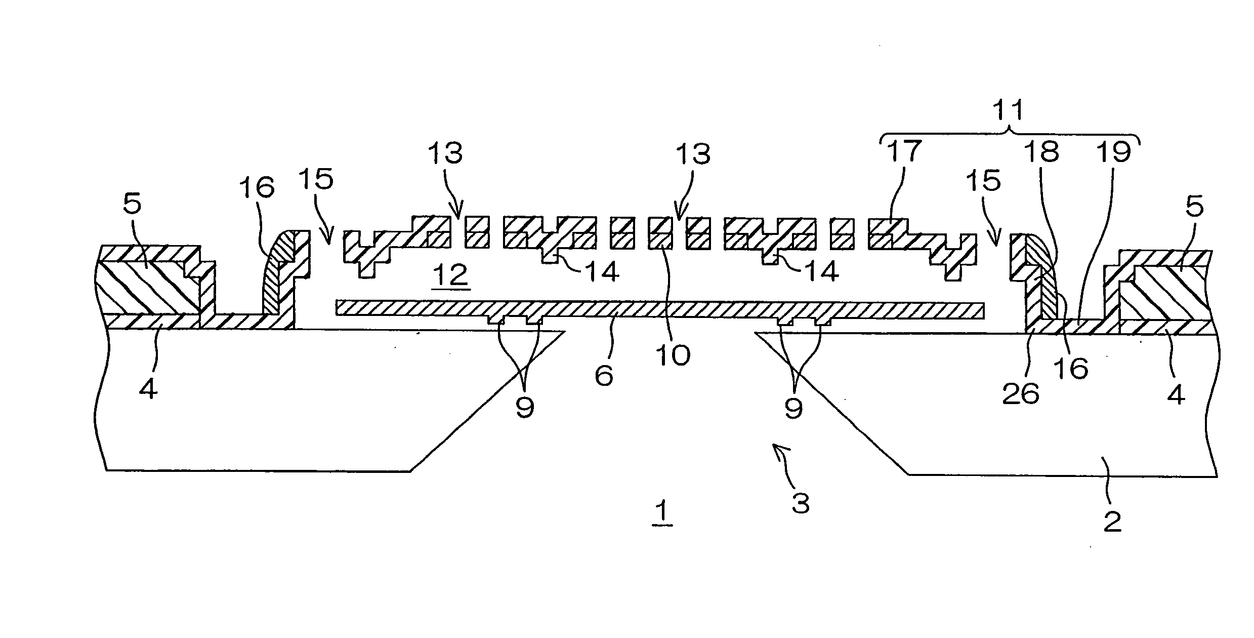
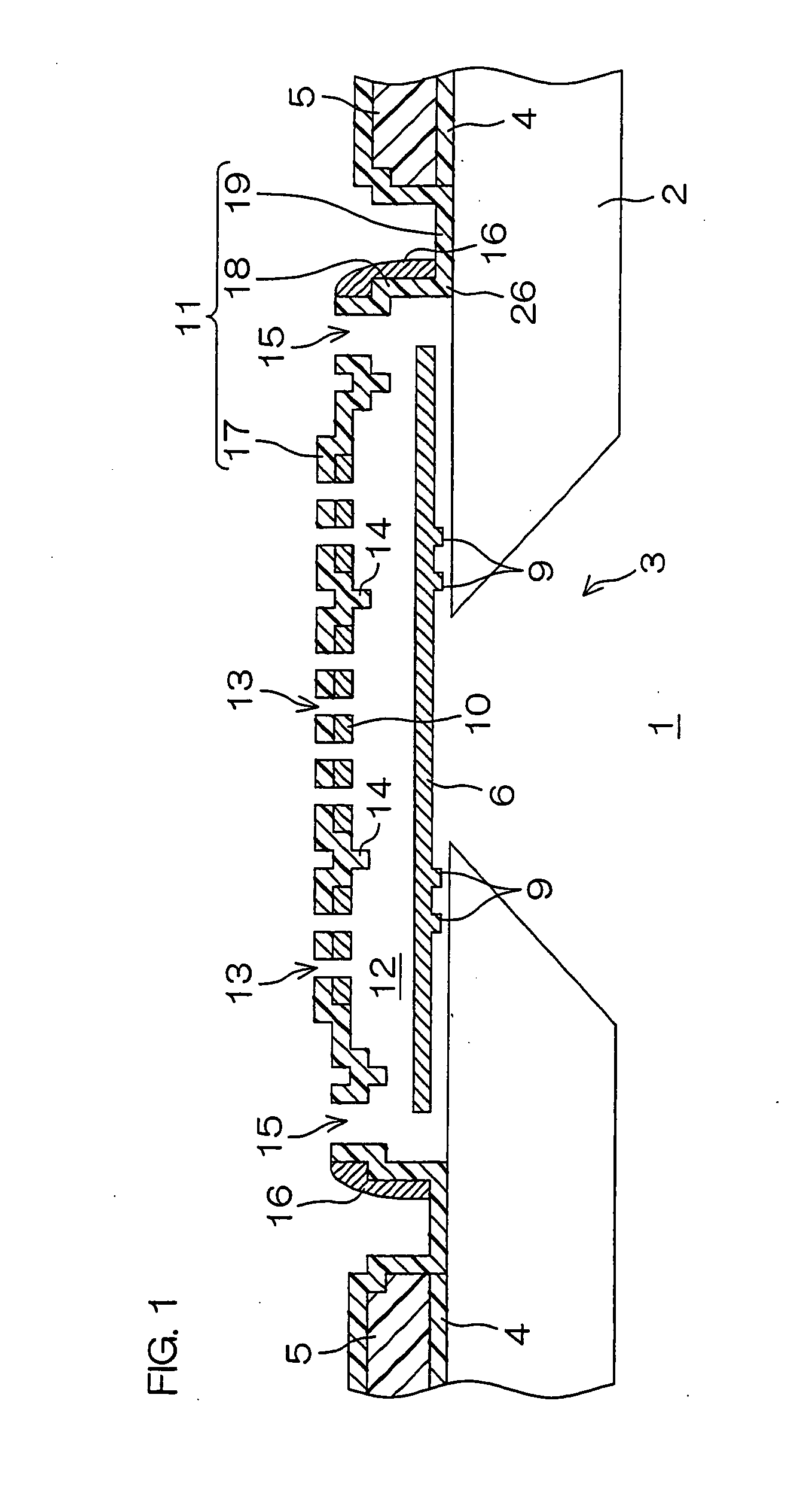
[0056]FIG. 1 is a schematic sectional view of a silicon microphone according to the present invention.

[0057]A silicon microphone 1 is a device (an MEMS device) manufactured according to the MEMS technique. The silicon microphone 1 includes a silicon substrate 2. A sound hole 3 (a through-hole) passing through the silicon substrate 2 from a second side (from the side of the back surface) toward a first side (toward the side of the front surface) and having a trapezoidal sectional shape narrowed toward the first side (spreading toward the second side) is formed in a central portion of the silicon substrate 2.

[0058]A first insulating film 4 is laminated on the silicon substrate 2. The first insulating film 4 is made of silicon oxide, for example.

[0059]A second insulating film 5 is laminated on the first insulating film 4. The second insulating film 5 is made of PSG (Phospho Silicate Glass), for example.

[0060]The first insulating film 4 and the second insulating film 5 are partially rem...

second embodiment

[0092]FIG. 3 is a schematic sectional view of a silicon microphone according to the present invention. FIG. 4 is a schematic plan view of a diaphragm shown in FIG. 3.

[0093]A silicon microphone 31 includes a silicon substrate 32. A sound hole 33 having a trapezoidal sectional shape narrowed toward the side (a first side) of the upper surface (spreading toward the lower surface) is formed in the silicon substrate 32. A first insulating film 34 is laminated on the silicon substrate 32. The first insulating film 34 is made of silicon oxide, for example.

[0094]A second insulating film 35 is laminated on the first insulating film 34. The second insulating film 35 is made of silicon nitride, for example.

[0095]The first insulating film 34 and the second insulating film 35 are partially removed from the sound hole 33 and a portion (hereinafter referred to as a “through-hole peripheral portion”) of the upper surface of the silicon substrate 32 located around the sound hole 33. Thus, the throug...


PUM


Abstract

The method of etching a sacrificial layer according to the present invention includes the steps of forming a sacrificial layer having a protrusive shape on a base layer, forming a covering film covering the sacrificial layer, forming a protective film made of a material whose etching selection ratio to the sacrificial layer is greater than the etching selection ratio of the covering film to the sacrificial layer on a portion of the covering film opposed to the side surface of the sacrificial layer, and etching the sacrificial layer after the formation of the protective film.

Description

BACKGROUND OF THE INVENTION[0001]1. Field of the Invention[0002]The present invention relates to a method of etching a sacrificial layer, a method of manufacturing an MEMS device with the etching method and an MEMS device manufactured according to the manufacturing method, as well as an MEMS sensor.[0003]2. Description of Related Art[0004]A device to which an MEMS (Micro Electro Mechanical Systems) technique is applied has been recently loaded on a portable telephone or the like, and hence an MEMS device is increasingly watched with interest. For example, a silicon microphone is known as a typical MEMS device.[0005]FIGS. 6A to 6I are schematic sectional views showing a method of manufacturing a conventional silicon microphone in step order.[0006]In order to manufacture the conventional silicon microphone, a thermal oxide film 111 and a thermal oxide film 121 are first formed on a first surface and a second surface of a silicon substrate 102 by thermal oxidation, as shown in FIG. 6A....

Claims


Application Information

Patent Timeline
Patent Type & Authority Applications(United States)
IPC IPC(8): H01L29/84H01L21/306H01L29/06
CPCB81B2201/0257B81C1/00476B81C1/00801H04R31/00H01L28/40H04R19/005H04R19/04B81C2201/053
Inventor NAKATANI, GORO
Owner ROHM CO LTD
Why Eureka
Try Eureka