Solid-state imaging device and method for manufacturing the same

a solid-state imaging and imaging device technology, applied in the direction of radioation control devices, television system scanning details, television systems, etc., can solve the problems of color mixing and shading, difficult to accurately condense incident light onto the photodiode, and other types of cmos-type solid-state imaging devices inherently have problems, so as to improve the incidence efficiency and reduce the profile. , the effect of reducing the number o

Inactive Publication Date: 2010-03-18
FUJIFILM CORP
View PDF2 Cites 7 Cited by
  • Summary
  • Abstract
  • Description
  • Claims
  • Application Information

AI Technical Summary

Benefits of technology

[0018]A solid-state imaging device provided with a signal reading circuit formed of a MOS transistor is configured so that global wiring layers of a multi-layered structure are formed on a semiconductor substrate on which photodiodes and signal reading circuits are formed, and that optical layers such as a color filter and microlens are stacked thereon. Therefore, a distance traveled by incident light until it reaches the photodiodes after passing through the microlens and the color filter layer becomes long. Multiple reflections, lowering in light condensing efficiency, color mixing, shading, and lowering the profile would occur.
[0019]The present invention provides a solid-state imaging device capable of increasing the incidence efficiency and avoiding color mixing and shading, by reducing multiple reflections of incident light due to global wirings and attempting to make a profile of the solid-state imaging device be lower. The invention also provides a method for manufacturing the solid-state imaging device.
[0022]Accordingly, since a metal wiring layer equivalent to one layer of a multi-layered structure used in a related art is changed to a high-concentration impurity diffused layer, a lower profile can be achieved.
[0023]According to the above configuration and method, wirings formed of the high-concentration impurity diffused layer above the semiconductor substrate is used as global wirings. Therefore, a solid-state imaging device having a lower profile can be achieved. Thereby, multiple reflections of incident light due to the global wirings can be reduced, the incidence efficiency can be improved by a further lower profile, and it becomes possible to avoid color mixing and shading.

Problems solved by technology

Also, since the microlens 16 is away from the n region 3a constituting the photodiode, it becomes difficult to accurately condense the incident light onto the photodiode, which may cause color mixing and shading.
Also, CMOS type solid-state imaging devices of other types inherently have problems such as lowering in light condensing efficiency, color mixing and shading, which are caused by multiple reflections due to multi-layered wirings and a long distance between the microlenses and the photodiodes.

Method used


Image

  • Solid-state imaging device and method for manufacturing the same
  • Solid-state imaging device and method for manufacturing the same
  • Solid-state imaging device and method for manufacturing the same

Examples


Embodiment Construction

[0051]Hereinafter, embodiments of the present invention will be described with reference to the accompanying drawings.

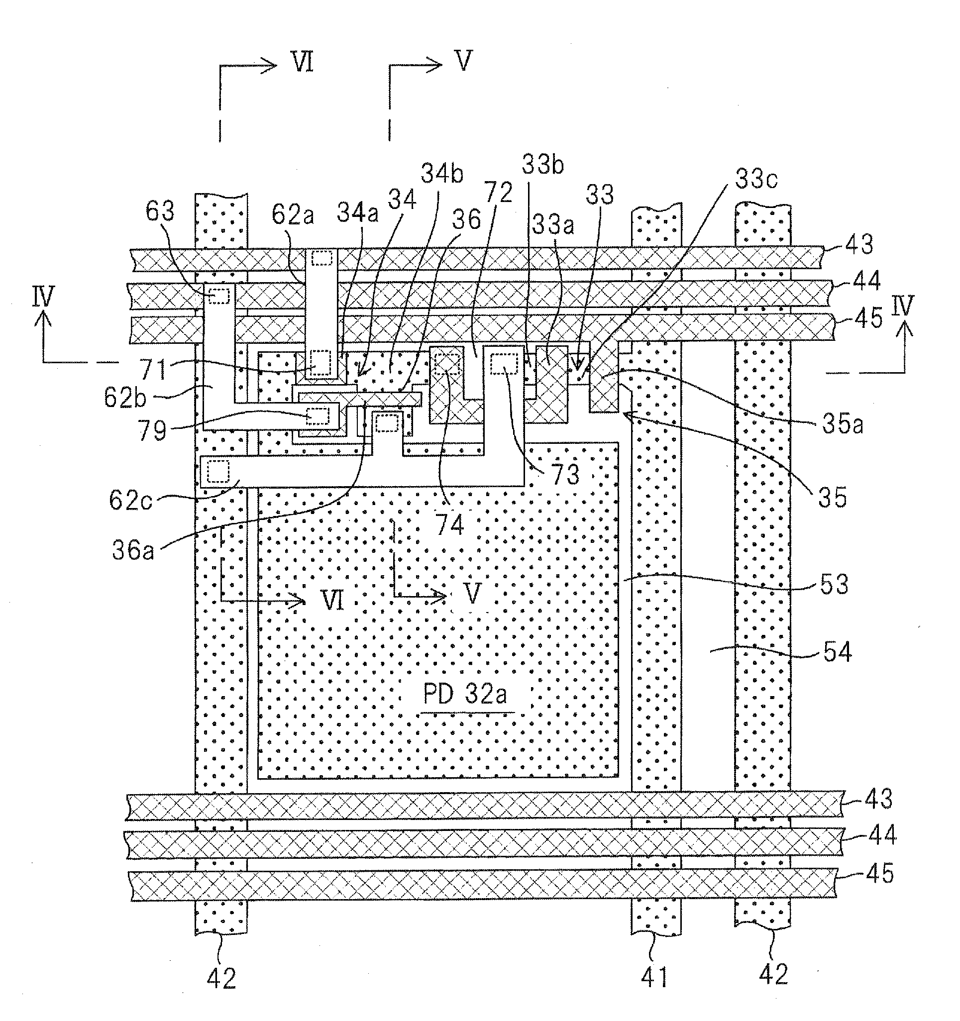
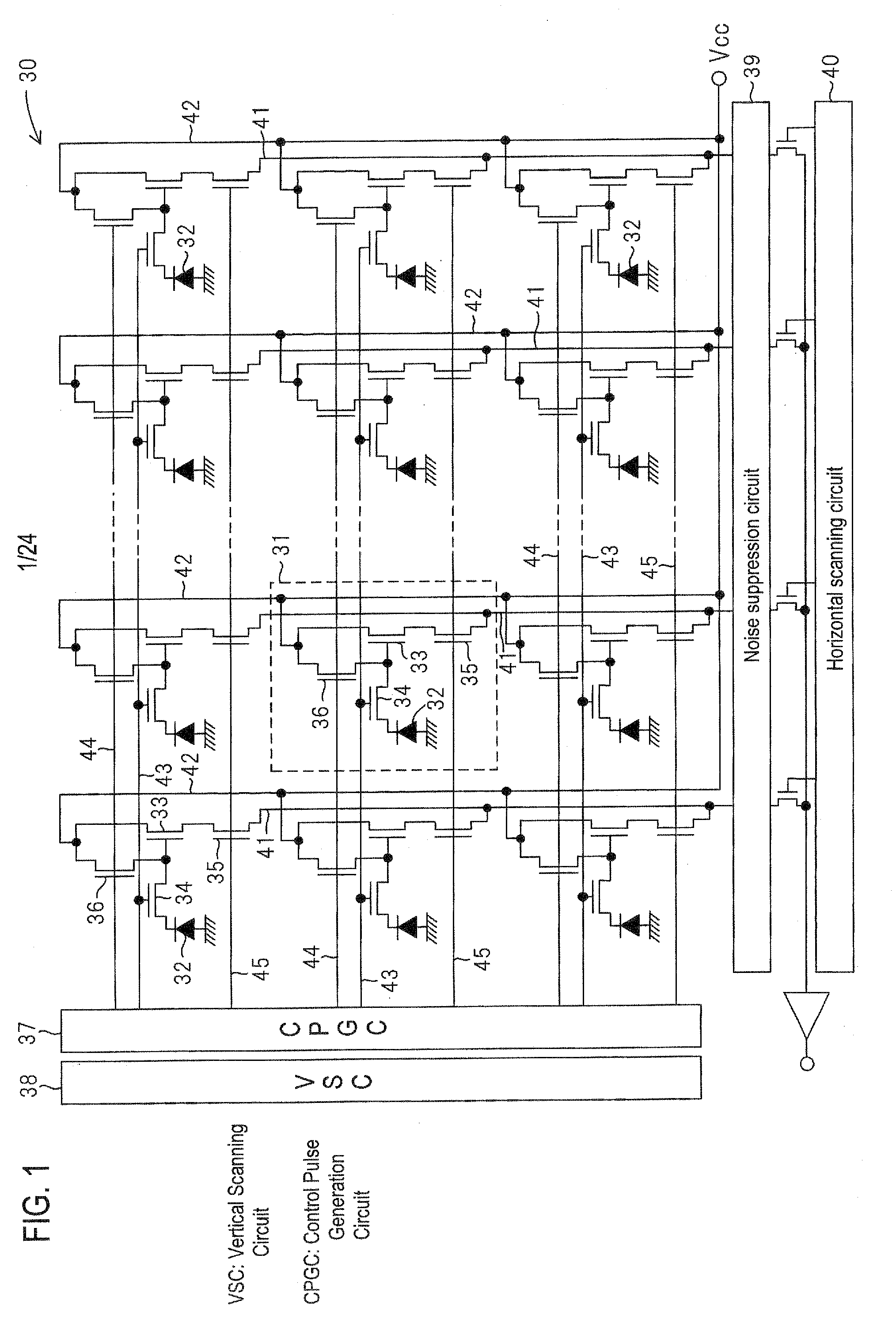
[0052]FIG. 1 is a circuit diagram of a CMOS type solid-state imaging device according to an embodiment of the invention. In the CMOS type solid-state imaging device 30 according to this embodiment, a plurality of unit pixels 31 are formed and arranged in a two-dimensional grid form (in the illustrated example, in the form of a square lattice) on a light-receiving surface (image area) of a semiconductor substrate. Each unit pixel 31 is provided with a photodiode 32 for detecting signal charges corresponding to an amount of received light and a signal reading circuit which will described later. The signal reading circuit reads captured image signals corresponding to the charges accumulated in the photodiode 32, and includes four transistors (33, 34, 35, and 36).

[0053]A control pulse generation circuit (CPGC) 37, a vertical scanning circuit (VSC) 38, a noise suppression...


PUM


Abstract

A solid-state imaging device includes plural photosensitive elements 32, signal reading circuits and first type wiring 41 and 42. The photosensitive elements 32 are formed and arranged in a two-dimensional array state ion a light-receiving portion area of a semiconductor substrate 50. The signal reading circuits are formed so as to correspond to the respective photosensitive elements 32. Each signal reading circuit detects a captured image signal corresponding to signal charges of the photosensitive elements 32. The signal charges are accumulated in response to an amount of received light which comes from an object. The first type wiring 41 and 42 are formed of a high-concentration impurity diffused layer, are formed in one direction along a surface of the light-receiving portion area, and are connected to plural ones of the signal reading circuits which are provided along the one direction.

Description

CROSS-REFERENCE TO RELATED APPLICATIONS[0001]This application claims the benefit of Japanese Patent Application No. 2008-236642 filed Sep. 16, 2008, the entire contents of which are hereby incorporated by reference, the same as if set forth at length.BACKGROUND OF THE INVENTION[0002]1. Technical Field[0003]The present invention relates to a solid-state imaging device formed on a semiconductor substrate and a method for manufacturing the same.[0004]2. Related Art[0005]FIG. 22A is a schematic surface view of a CMOS type solid-state imaging device of a related art in which a plurality of photodiodes (photoelectric conversion elements: photosensitive elements) are arranged in a grid form on a light-receiving surface (image area) of the surface of a semiconductor substrate, and FIG. 22B is a circuit diagram of the CMOS type solid-state imaging device. The CMOS type solid-state imaging device 1 shown in the figures has a large number of unit pixels 3 which are formed and arranged on the i...

Claims


Application Information

Patent Timeline
Patent Type & Authority Applications(United States)
IPC IPC(8): H04N5/335H01L31/18H01L27/146H04N5/357H04N5/369H04N5/374H04N5/3745
CPCH01L27/14623H01L27/14636H04N5/378H01L27/14818H04N5/37452H01L27/14685H04N25/771H04N25/75
Inventor SIZUKUISI, MAKOTO
Owner FUJIFILM CORP
Why Eureka
Try Eureka