Eureka AIR delivers breakthrough ideas for toughest innovation challenges, trusted by R&D personnel around the world.

Semiconductor Device and Method for Manufacturing the Same

Inactive Publication Date: 2010-03-18
DONGBU HITEK CO LTD
View PDF10 Cites 2 Cited by
  • Summary
  • Abstract
  • Description
  • Claims
  • Application Information

AI Technical Summary

Benefits of technology

[0015]An object of the present invention is to provideone or more methods for manufacturing a semiconductor device that reduces or avoids byproduct deposition on a metal line when etching a hard mask.
[0018]The method(s) for manufacturing a semiconductor device according to the present invention may prevent the generation of byproduct when etching a hard mask (e.g., for etching a metal line having a pitch of 120 nm or less), without the requirement of a subsequent cleaning process. Thus, the presently disclosed methods simplify and reduce the costs of a semiconductor manufacturing process.

Problems solved by technology

Thus, an undesired byproduct may be generated during the step of etching the oxide mask 22.
The polymer remains on exposed surfaces (e.g., a top or side) of each metal line, which may increase surface resistance, and reduce reliability and device yield.

Method used


Image

  • Semiconductor Device and Method for Manufacturing the Same
  • Semiconductor Device and Method for Manufacturing the Same
  • Semiconductor Device and Method for Manufacturing the Same

Examples


Embodiment Construction

[0027]Reference will now be made in detail to the specific embodiments of the present invention, examples of which are illustrated in the accompanying drawings. Wherever possible, the same reference numbers will be used throughout the drawings to refer to the same or like parts.

[0028]FIGS. 2a to 2e are cross-sectional views illustrating exemplary structures made during a method for manufacturing a semiconductor device according to exemplary embodiments of the present invention.

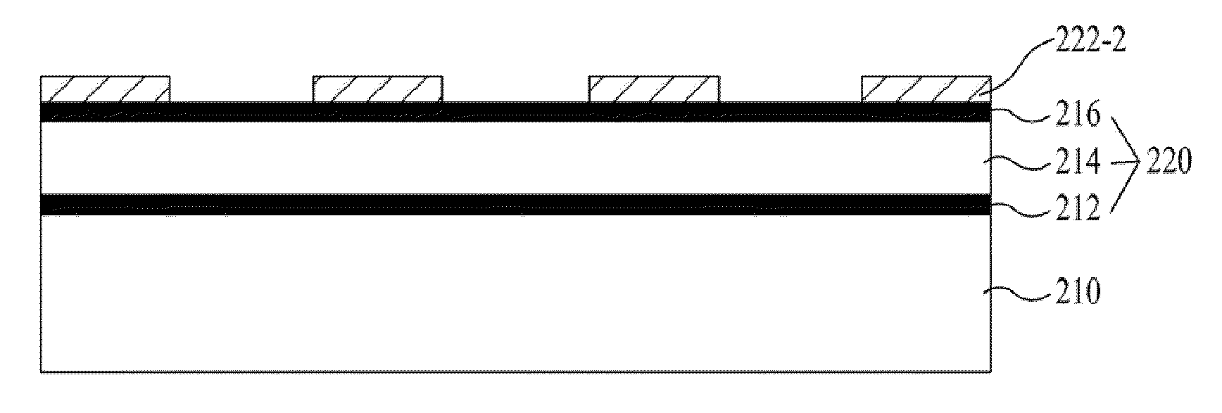
[0029]As shown in FIG. 2a, a back end process method for manufacturing a semiconductor device according to exemplary embodiments of the present invention includes depositing a first TiN / Ti thin film 212 on a substrate 200. An aluminum (Al) layer 214 can then be deposited on or over the first TiN / Ti thin film 212. A second TiN / Ti thin film 216 may then be deposited on or over the aluminum layer 214. The first and second TiN / Ti thin films form diffusion barriers for the aluminum layer 214. Generally, each TiN / Ti...


PUM


Abstract

The present method for manufacturing a semiconductor device comprises the steps of forming an aluminum wiring layer on a substrate; sequentially forming a hard mask, a polysilicon layer, and a bottom anti-reflective coating over the aluminum wiring layer; etching the polysilicon layer using a photoresist pattern formed over the bottom anti-reflective coating as mask; etching the hard mask to a predetermined thickness; and etching the hard mask to expose the aluminum wiring layer. The method for manufacturing a semiconductor device according to the present invention may prevent byproducts and polymer residue from when patterning the hard mask. As a result, the presently disclosed methods may avoid the need for a conventional cleaning process prior to etching the aluminum wiring layer to form aluminum lines.

Description

CROSS REFERENCE TO RELATED APPLICATION[0001]This application claims the benefit of the Patent Korean Application No. 10-2008-0090717, filed on 16 Sep. 2008, which is hereby incorporated by reference as if fully set forth herein.BACKGROUND OF THE DISCLOSURE[0002]1. Field of the Disclosure[0003]The present invention relates to a semiconductor device, more particularly, to a semiconductor device and a method for manufacturing the device.[0004]2. Discussion of the Related Art[0005]In general, an etching mask is used to form a desired pattern. As the pitch of a metal wiring gets smaller (e.g., 120 nm or less), the thickness of a photoresist may be limited. To solve this limitation, a double mask structure using a thin layered oxide mask can be used.[0006]FIG. 1a is a sectional view illustrating a conventional method for manufacturing semiconductor device.[0007]In reference to FIG. 1a, according to a conventional back end process for forming metal lines, a first titanium nitride / titanium ...

Claims


Application Information

Patent Timeline
IPC IPC(8): H01L21/3205
CPCH01L21/2855H01L21/28556H01L21/7685H01L21/31116H01L21/32139H01L21/28562
Inventor YUN, KI JUN
Owner DONGBU HITEK CO LTD
Why Eureka
Eureka Blog
Learn More