Waiver mechanism for physical verification of system designs

a technology of physical verification and system design, applied in the field of circuit design verification, can solve the problems of ip received by the soc designer lacking layer identification and/or incomplete verification of the ip, circuit design getting larger and more complex at the 90 nanometer and smaller technology nodes,

Inactive Publication Date: 2010-03-18
BELL SEMICON LLC
View PDF19 Cites 7 Cited by
  • Summary
  • Abstract
  • Description
  • Claims
  • Application Information

AI Technical Summary

Benefits of technology

[0004]The objects, features and advantages of the present invention include providing a method and / or apparatus for implementing a waiver mechanism for physical verification of system designs that may (i) provide a waiver mechanism schema to reduce a number of system level verification failures, (ii) remove acceptable verification errors from consideration during development, (iii) optimize a design workflow, (iv) optimize a verification workflow, (v) identify and distinguish errors that are IP level versus top level design specific and / or (vi) ensure that the top-level design errors are fixed via automated and / or manual means.

Problems solved by technology

Circuit designs are getting larger and more complex at the 90 nanometer and smaller technology nodes.
Because the time to market is shrinking with advancements in technology and product innovation, design teams struggle with meeting tight schedules and remaining under budget.
For example, the IP received by the SoC designers may lack layer-identifications and / or incomplete verification of the IP at the Graphic Data System II (GDSII) format level.
As the IP is being co-developed, some aspects of the IP have not been fully developed and / or validated.
Furthermore, a dynamic nature of process rule specifications create problems, whereby the place and route (i.e., design implementation) systems cannot keep pace and verification does not happen until the very end of the development cycle.

Method used


Image

  • Waiver mechanism for physical verification of system designs
  • Waiver mechanism for physical verification of system designs
  • Waiver mechanism for physical verification of system designs

Examples


Embodiment Construction

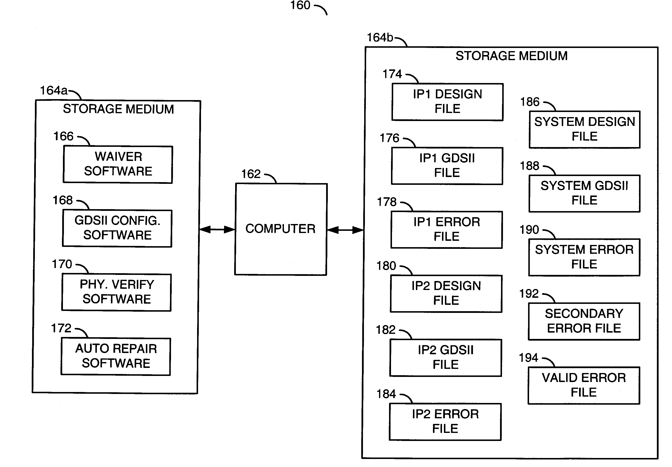
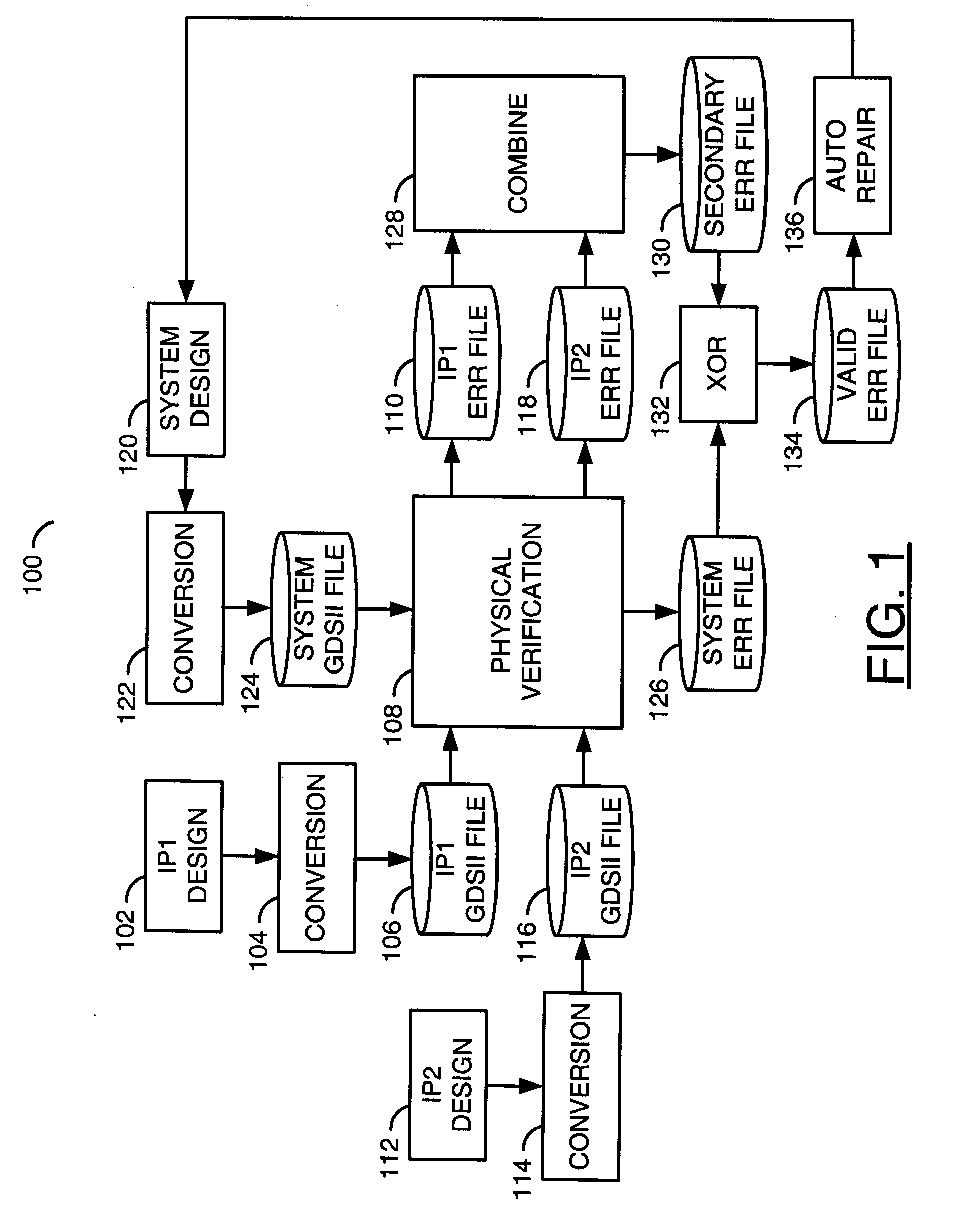
[0009]Referring to FIG. 1, a flow diagram of an example method 100 to waive physical verification failures in a system design is shown in accordance with a preferred embodiment of the present invention. The method (or process) 100 may be implemented as a software tool executable on a computer. The method 100 generally comprises a step (or block) 102, a step (or block) 104, a step (or block) 106, a step (or block) 108, a step (or block) 110, a step (or block) 112, a step (or block) 114, a step (or block) 116, a step (or block) 118, a step (or block) 120, a step (or block) 122, a step (or block) 124, a step (or block) 126, a step (or block) 128, a step (or block) 130, a step (or block) 132, a step (or block) 134 and a step (or block) 136.

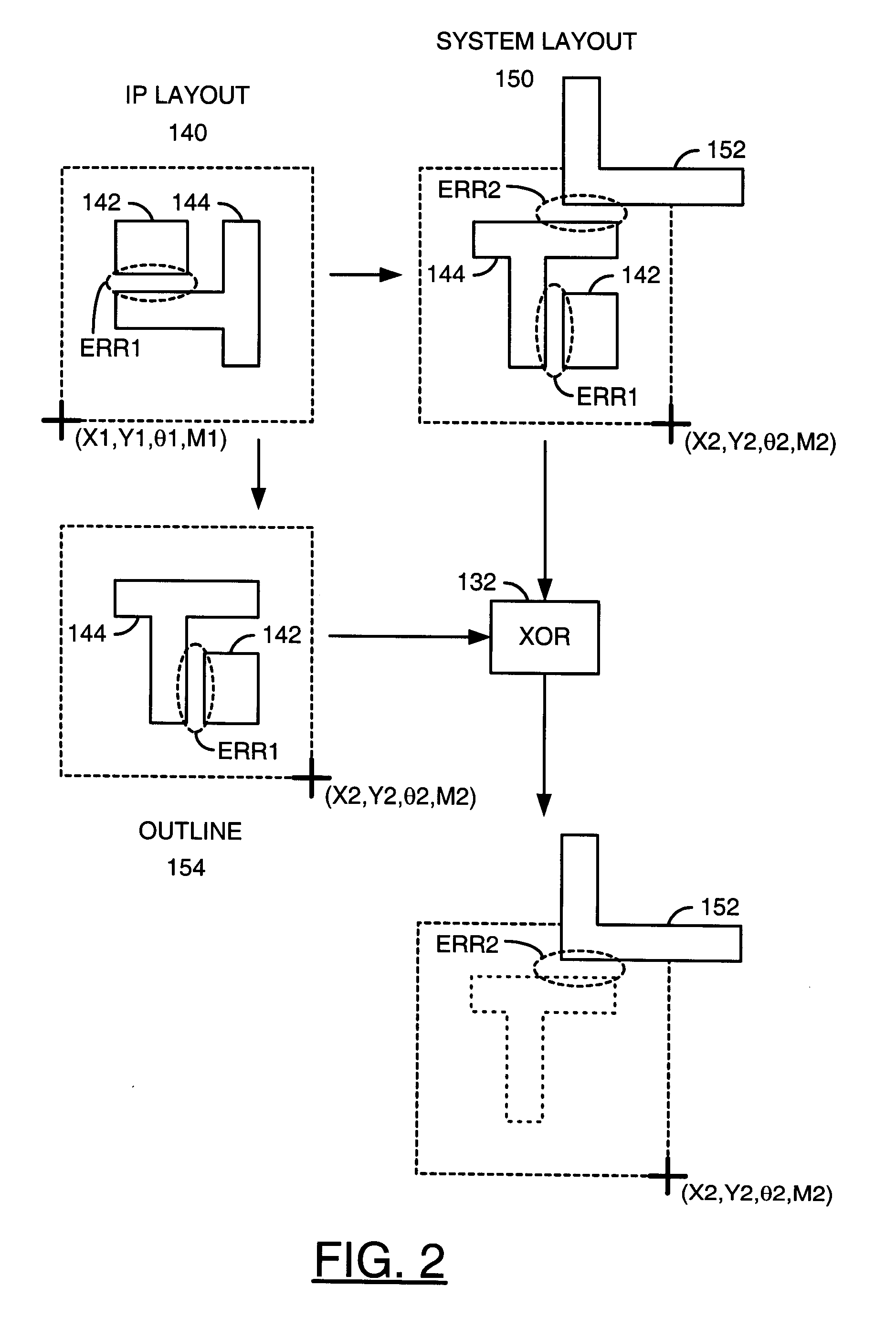
[0010]The method 100 is generally operational to “mask” and / or “waive” specific errors in Intellectual Property (IP) / blocks / macros and / or any sub-blocks / building blocks used for developing and / or implementing a System-On-a-Chip (SoC). The method may p...


PUM


Abstract

A method of waiving verification failures is disclosed. The method generally includes the steps of (A) generating a plurality of circuit error files by performing a plurality of physical verifications on a plurality of circuit designs, the circuit error files containing a plurality of circuit errors of the circuit designs, (B) generating a system error file by performing an additional physical verification on a system design, the system error file containing a plurality of system errors of the system design, the system design incorporating the circuit designs, (C) generating a valid error file by removing the circuit errors from the system error file, the valid error file containing a plurality of valid errors comprising a subset of the system errors and (D) storing the valid error file in a recording medium.

Description

FIELD OF THE INVENTION[0001]The present invention relates to circuit design checking generally and, more particularly, to a method and / or apparatus for implementing a waiver mechanism for physical verification of system designs.BACKGROUND OF THE INVENTION[0002]Circuit designs are getting larger and more complex at the 90 nanometer and smaller technology nodes. Because the time to market is shrinking with advancements in technology and product innovation, design teams struggle with meeting tight schedules and remaining under budget. Factoring in Intellectual Property (IP) co-development, a verification methodology that is able to service the criteria of a customer for both quality of results and turnaround time is desired. With IP co-development, not all building blocks for a System-On-a-Chip (SoC) design are available off-the-shelf during an SoC build and integration. As a result, an intelligent “waiver” mechanism for Design Rule Checks (DRCs) pertaining to the IP is often sought. T...

Claims


Application Information

Patent Timeline
Patent Type & Authority Applications(United States)
IPC IPC(8): G06F17/50
CPCG06F17/5081G06F30/398
Inventor LAKSHMANAN, VISWANATHANJOSEPHIDES, MICHAELMILLER, LISA M.
Owner BELL SEMICON LLC
Why Eureka
Try Eureka