Structure of solar cell panel and manufacturing method of electrode of solar cell panel

a manufacturing method and technology of solar cell panels, applied in the direction of photovoltaics, electrical devices, semiconductor devices, etc., can solve the problem of burden of silk sheet fabrication, and achieve the effect of saving time and production costs

Inactive Publication Date: 2010-03-25
GINTECH ENERGY CORPORATION
View PDF4 Cites 15 Cited by
  • Summary
  • Abstract
  • Description
  • Claims
  • Application Information

AI Technical Summary

Benefits of technology

[0008]One object of the present invention is to provide a pattern of a conductive electrode on a surface of a wafer via a laser beam, and the wafer is processed with an alloy treatment via the laser beam, so the above mentioned processes of screen printing and sintering are able to be disregarded, time and production cost are therefore saved.
[0009]Another object of the present invention is to provide an application of laser projection capable of rapidly modifying a pattern, so a customized pattern of a conductive electrode can be freely modified or changed, so customers have more pattern choices.
[0010]One another object of the present invention is to replace the screen printing process and the silk sheet fabrication with a laser beam capable of providing a pattern of a conductive electrode on a surface of a wafer, so manufacturing cost of small numbers of product or customized products is cut down to further lower the unit cost of each product.
[0011]One another object of the present invention is to reduce resistance value of a conductive electrode for raising efficiency of current yielding for a solar cell.

Problems solved by technology

The procedure of fabricating a silk sheet for screen printing is complex and time consuming and labor intensive, the cost, without a doubt, is high, so massive production has to be conducted to proportioning the fabrication cost to each finished product.
But for a small-amount production or for customized products, the cost of silk sheet fabrication is a burden for the proportioned production cost, therefore the averaging selling price (ASP) is not able to be lowered, a less competitiveness in the marketplace is occurred.

Method used


Image

  • Structure of solar cell panel and manufacturing method of electrode of solar cell panel
  • Structure of solar cell panel and manufacturing method of electrode of solar cell panel
  • Structure of solar cell panel and manufacturing method of electrode of solar cell panel

Examples


Embodiment Construction

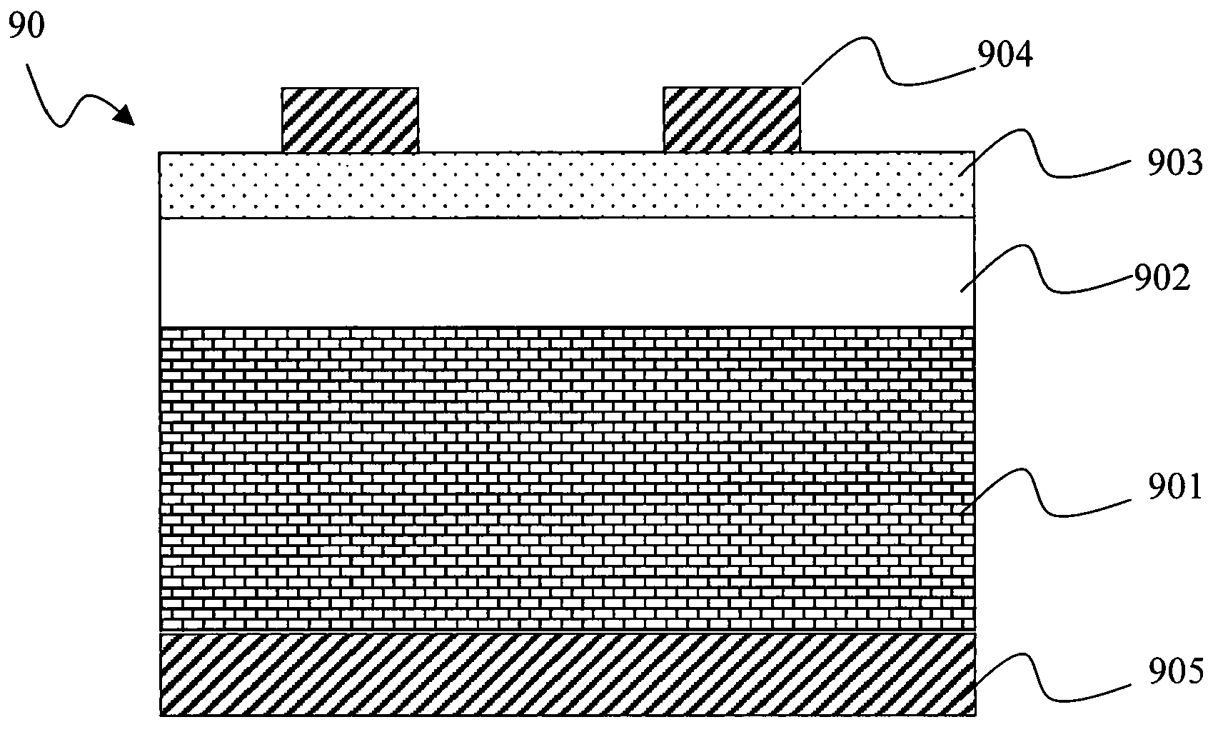
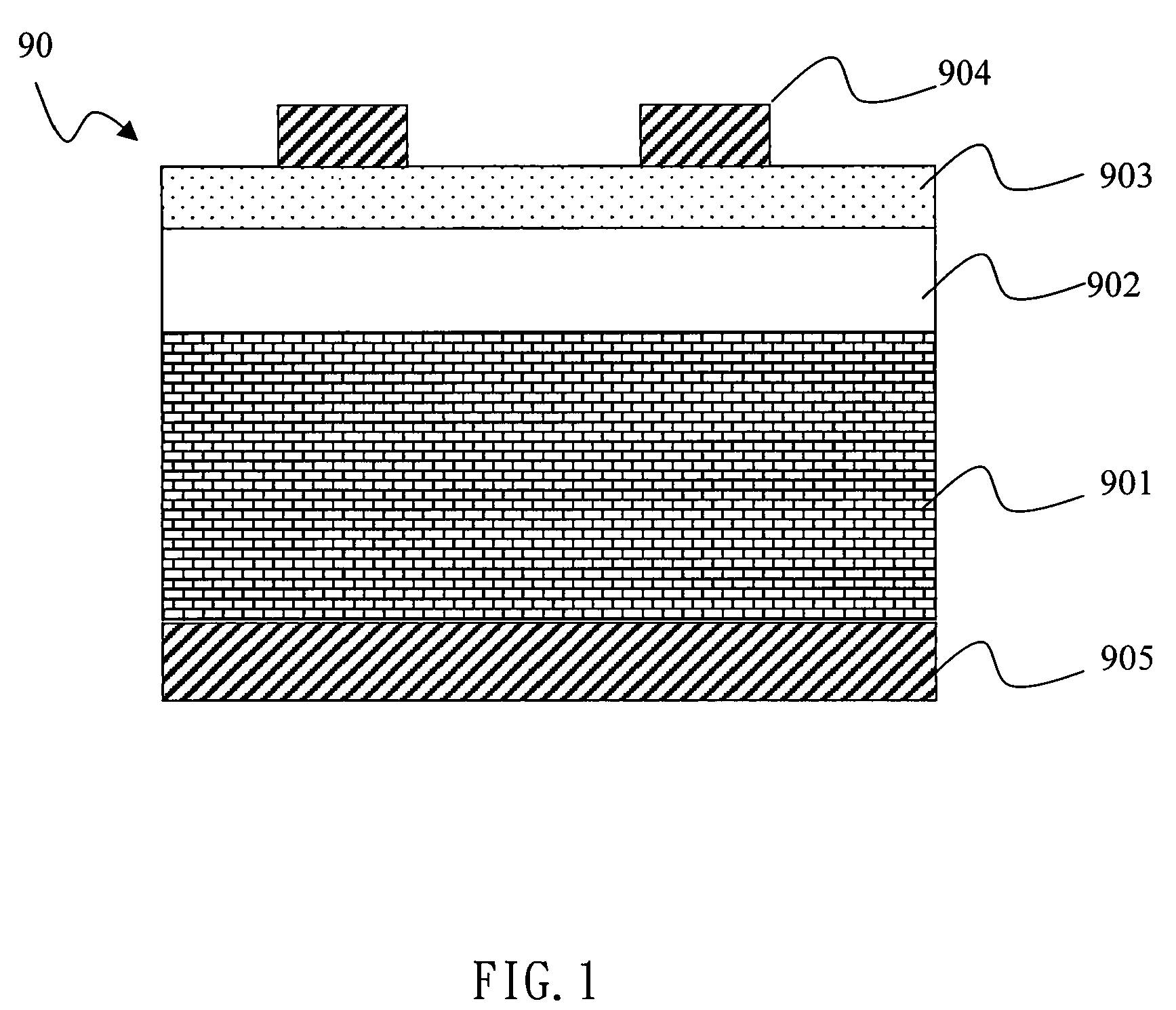
[0018]Hereinafter a structure of a first characteristic of the present invention covers or is provided on top of a second characteristic, this may include an embodiment wherein the first characteristic and the second characteristic are in direct contact, or include another embodiment wherein another characteristic is provided between the first characteristic and the second characteristic so the first characteristic and the second characteristic are not in direct contact.

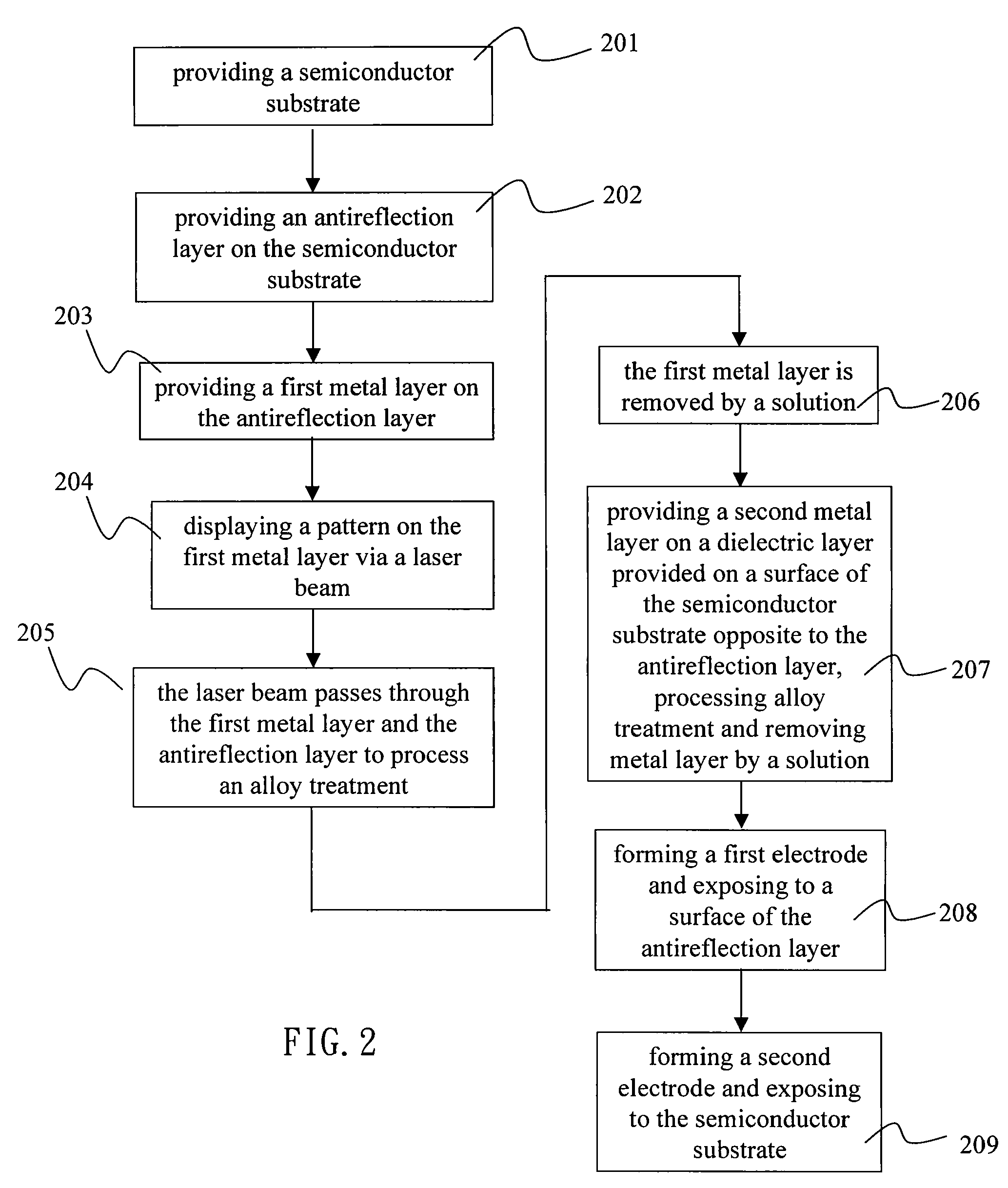
[0019]The described processes of screen printing and sintering are disregarded by the present invention, and the present invention discloses a solar cell panel and a manufacturing method of electrode of the panel, which applies a way of displaying an electrode pattern by a laser beam so as to form a metal silicide. That is, according to a desired pattern of the conductive electrode, a laser beam is emitted by a laser generating device and is projected on a surface of a wafer, and the lacer beam is controlled via vari...


PUM

PropertyMeasurementUnit
thicknessaaaaaaaaaa
contact resistanceaaaaaaaaaa
dielectricaaaaaaaaaa

Abstract

A manufacturing method of electrode of solar cell panel of the present invention comprises steps of providing a semiconductor substrate with an antireflection layer / a dielectric layer and a first metal layer in sequence, forming a first metal layer on the antireflection layer, projecting a pattern on the first metal layer by a laser beam to form a metal silicide on the semiconductor substrate in accordance with the outline of the pattern, removing the first metal layer by a chosen solution, forming a first electrode connecting to the metal silicide and exposed to a surface of the antireflection layer; and forming a second electrode on a surface of the semiconductor substrate opposite to the antireflection layer.

Description

RELATED APPLICATIONS[0001]This application claims priority to Taiwan Application Serial Number 97136116, filed Sep. 19, 2008, which is herein incorporated by reference.BACKGROUND[0002]1. Field of Invention[0003]The present invention relates to a manufacturing method of electrode of solar cell panel, more particularly to a manufacturing method of electrode of solar cell panel using desired patterns displayed with laser beam.[0004]2. Description of Related Art[0005]A conventional art of manufacturing a solar cell often includes the steps of: (1) crystal pulling process, silica is adopted as a main material, a crystal seed is placed in a crystal pulling furnace for obtaining an ingot; (2) edge trimming process, a wafer used in general micro electronic industries is that the ingot is directly processed with a cutting operation, but for a solar cell, plural chips are arranged as a rectangular matrix, in order to tighten the rectangular matrix, the ingot is often trimmed to a rectangular ...

Claims


Application Information

Patent Timeline
Patent Type & Authority Applications(United States)
IPC IPC(8): H01L31/052H01L21/00
CPCH01L31/022425Y02E10/50H01L31/18
Inventor CHANG, KAI-SHENGOU, NAI-TIENCHEN, TIEN-SZU
Owner GINTECH ENERGY CORPORATION
Why Eureka
Try Eureka