Active matrix substrate
a technology of active matrix and substrate, which is applied in the direction of instruments, semiconductor devices, electrical apparatus, etc., can solve the problems of inability to achieve a higher definition and small width in the y direction, and achieve the effect of suppressing the occurrence of line defects and improving the definition of display
- Summary
- Abstract
- Description
- Claims
- Application Information
AI Technical Summary
Benefits of technology
Problems solved by technology
Method used
Image

Examples
embodiment 1
[0097]A first embodiment of an active matrix substrate according to the present invention will now be described.
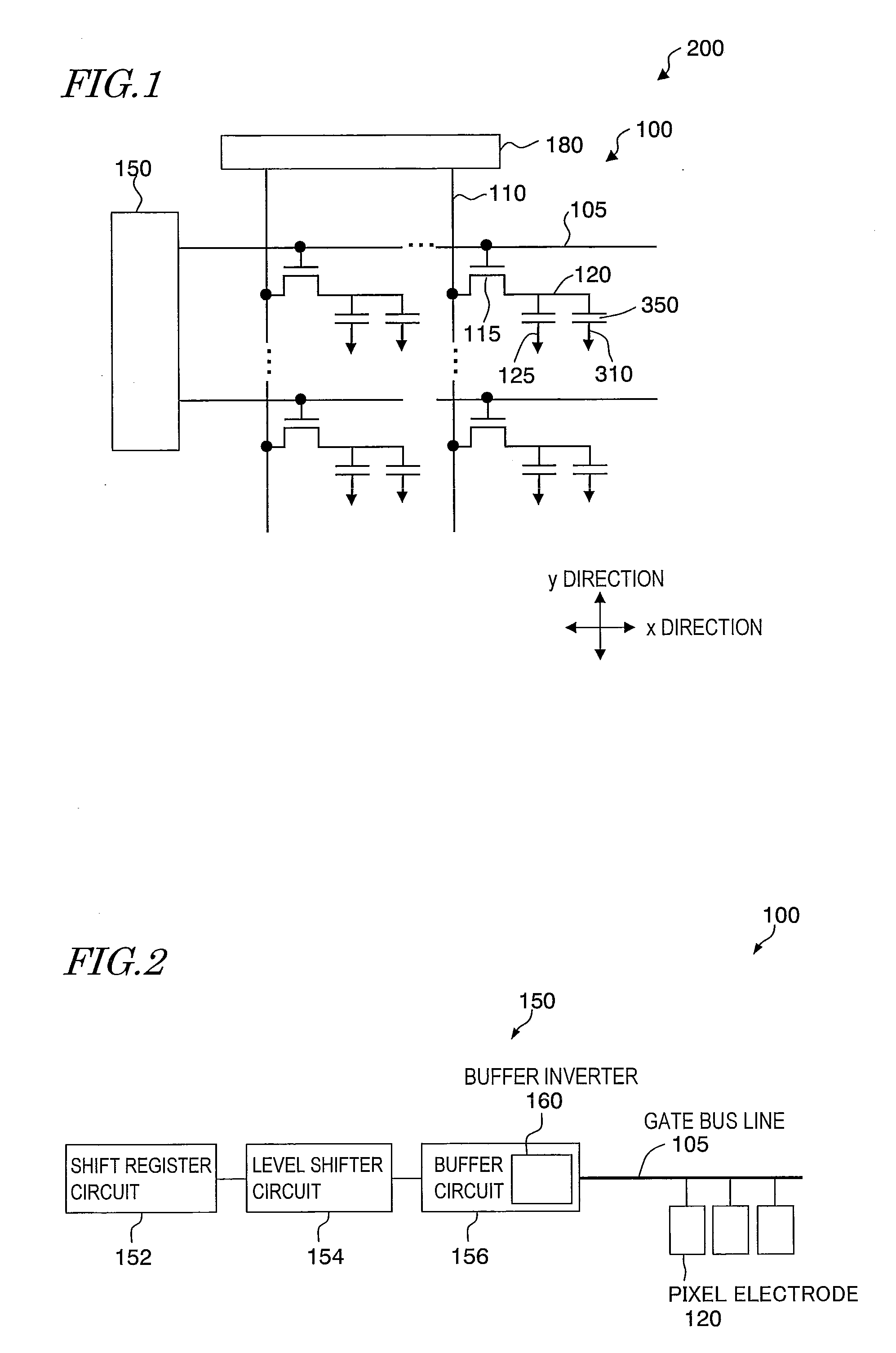
[0098]FIG. 1 shows an equivalent circuit of a display device 200 using an active matrix substrate 100 of the present embodiment. Herein, the display device 200 is a liquid crystal display device, and the display device 200 includes the active matrix substrate 100, a counter substrate (not shown) including a counter electrode 310, and a liquid crystal layer 350 placed between the counter substrate and the active matrix substrate 100.
[0099]The active matrix substrate 100 includes a gate bus line 105, a source bus line 110, a thin film transistor (TFT) 115, a pixel electrode 120, a storage capacitor line 125, a gate driver 150, and a source driver 180. There are a plurality of the pixel electrodes 120 arranged in a matrix pattern extending in the row direction (the x direction) and the column direction (the y direction), and the TFT 115 is provided for each pixel electrode. T...
embodiment 2
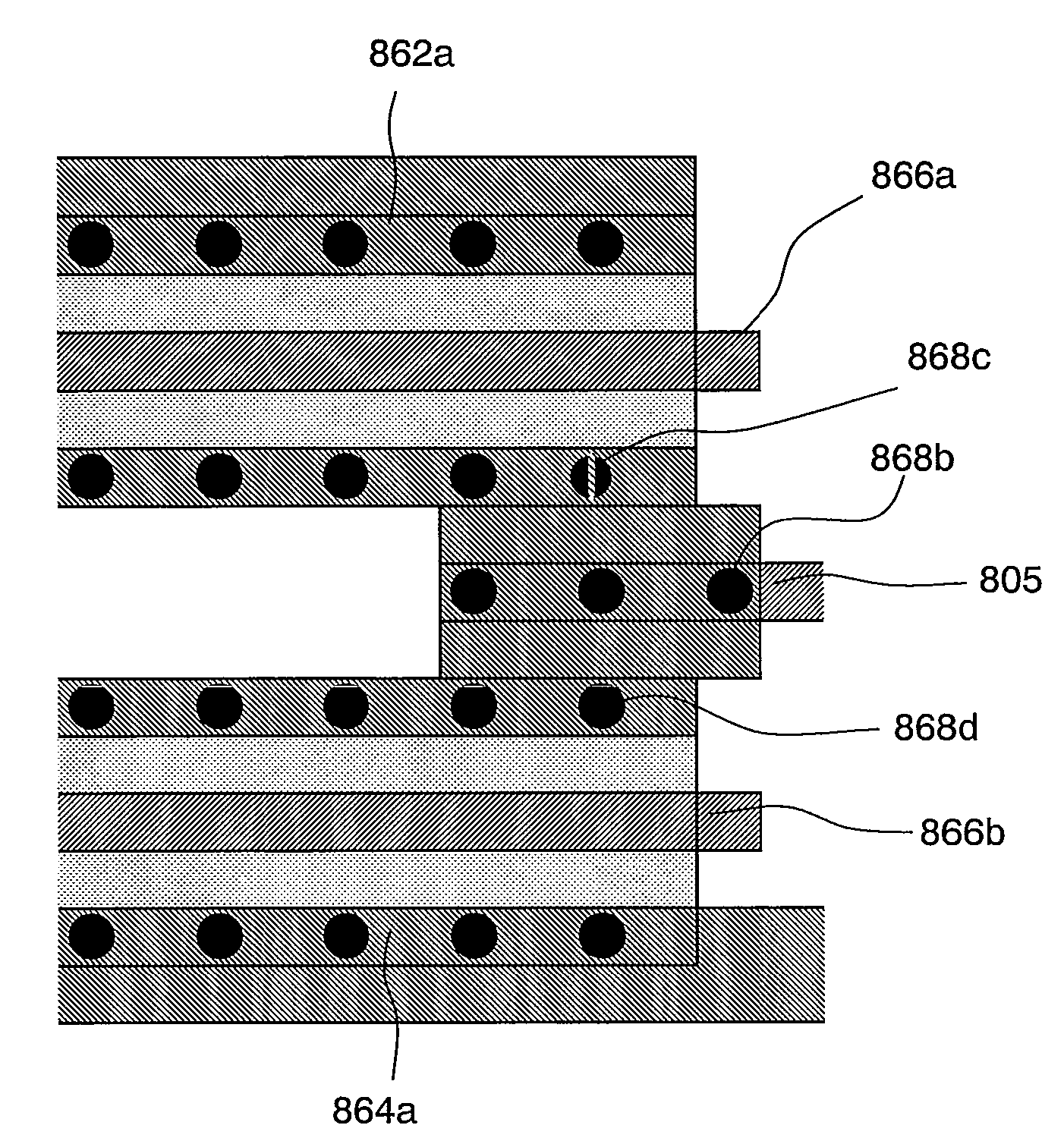
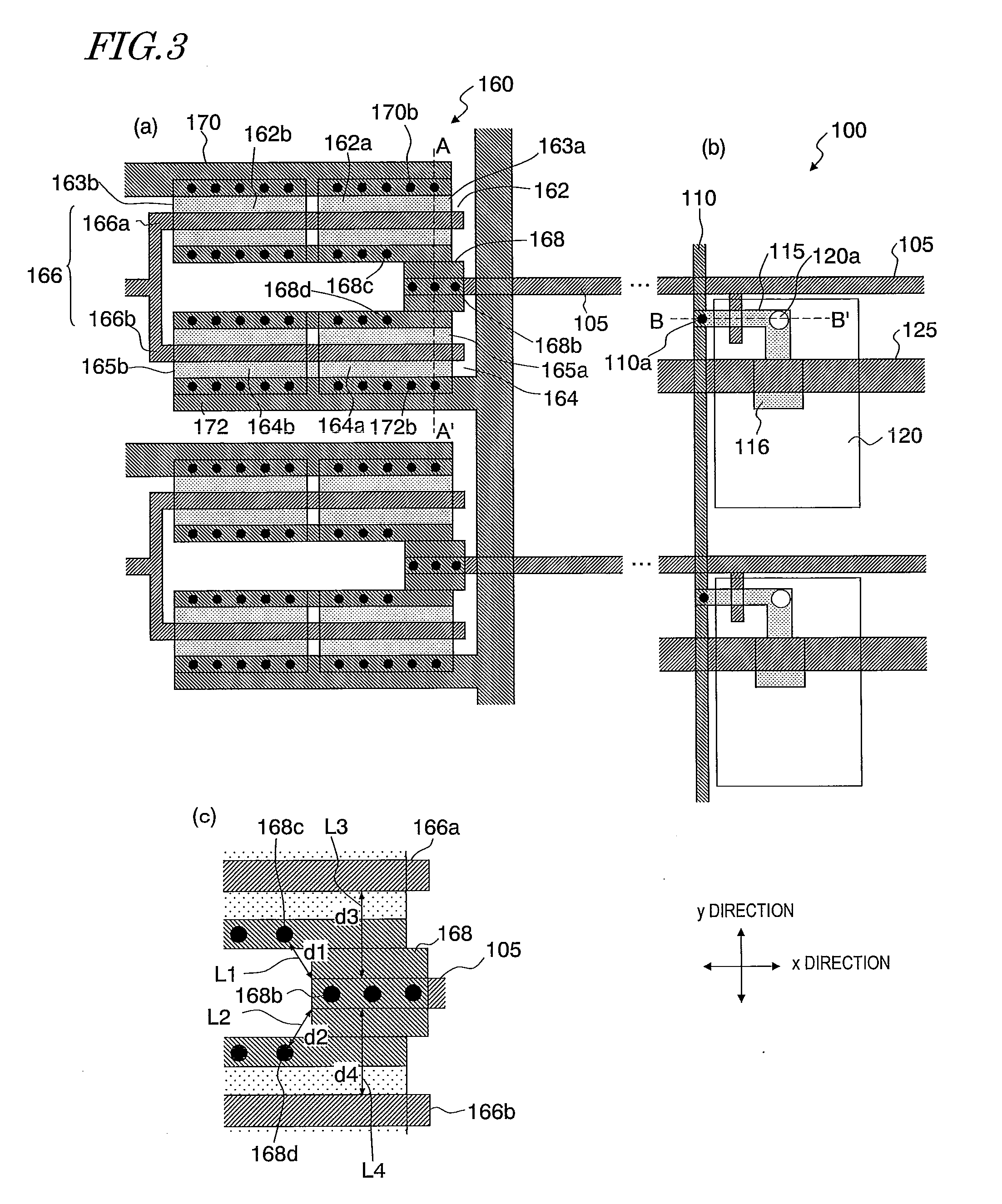
[0126]In the active matrix substrate of Embodiment 1, the gate bus line 105 overlaps the gate electrode 166 in the x direction, and the direction of the straight lines L3 and L4 denoting the shortest distances d3 and d4 between the gate electrode 166 and the gate bus line 105 is the y direction. However, the present invention is not limited to this.
[0127]Referring now to FIG. 5, a second embodiment of an active matrix substrate according to the present invention will be described. FIG. 5(a) shows a schematic plan view of the gate bus line 105 and the vicinity thereof in the peripheral region of the active matrix substrate 100 of the present embodiment, FIG. 5(b) shows a schematic plan view of one pixel electrode 120 and the vicinity thereof in the display region, and FIG. 5(c) shows an enlarged view of the contact portion 168 shown in FIG. 5(a) and the vicinity thereof. The active matrix substrate 100 of the present embodiment has substantially the similar configuration as that of t...
PUM
 Abstract
Description
Claims
Application Information
 - R&D
- Intellectual Property
- Life Sciences
- Materials
- Tech Scout
- Unparalleled Data Quality
- Higher Quality Content
- 60% Fewer Hallucinations
Browse by: Latest US Patents, China's latest patents, Technical Efficacy Thesaurus, Application Domain, Technology Topic, Popular Technical Reports.
© 2025 PatSnap. All rights reserved.Legal|Privacy policy|Modern Slavery Act Transparency Statement|Sitemap|About US| Contact US: help@patsnap.com