Semiconductor package system with through silicon via interposer

a technology of silicon via interposer and semiconductor, applied in the field of semiconductor package system, can solve problems such as reducing the device density of the package, increasing the length and width of the package, and routing problems,

Active Publication Date: 2010-04-01
STATS CHIPPAC LTD
View PDF16 Cites 113 Cited by
  • Summary
  • Abstract
  • Description
  • Claims
  • Application Information

AI Technical Summary

Problems solved by technology

When multiple chips are mounted within the same semiconductor package, routing problems may arise due to the different routing design of each individual chip.
This edge connection on laminated substrate, however, increases the length and width of the package and thus decreases the device density of the package.
The current laminated substrate has limited pitch capability.
Typically the laminated substrate can only accommodate semiconductor chips that are not designed for 3D interconnections.
In these new technology developments, laminated substrate proves to be inadequate for the modern need of semiconductor 3D interconnections.
Solutions to these problems have been long sought but prior developments have not taught or suggested any solutions and, thus, solutions to these problems have long eluded those skilled in the art.

Method used


Image

  • Semiconductor package system with through silicon via interposer
  • Semiconductor package system with through silicon via interposer
  • Semiconductor package system with through silicon via interposer

Examples


first embodiment

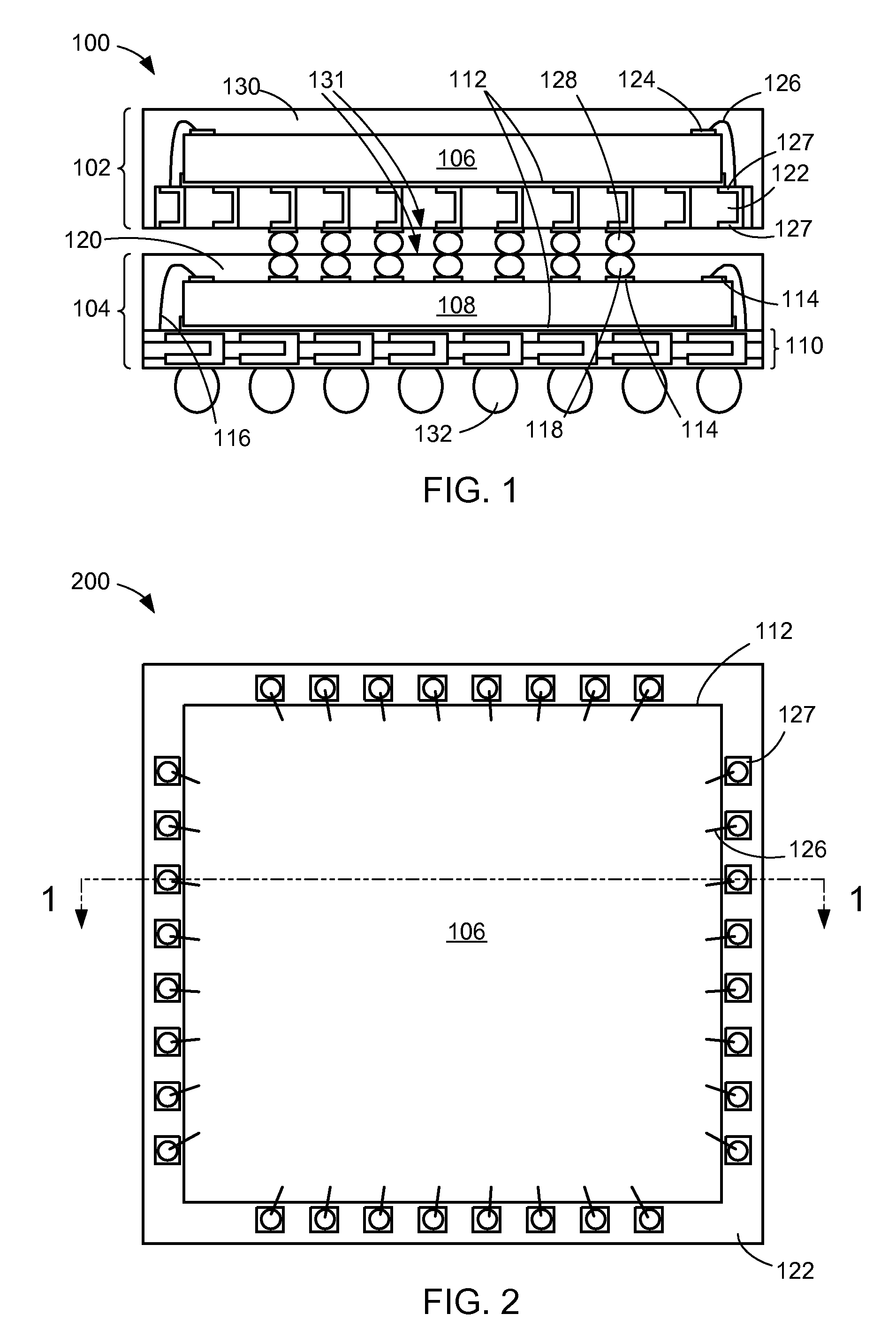
[0053]Referring now to FIG. 2, therein is shown a top view of an unfinished semiconductor package 200 of the present invention after an intermediate stage of the process. This top view is shown after the top die mold 130 in FIG. 1 has been removed. The top semiconductor die 106 is shown and the die paste layer 112 is also shown. The through silicon via interposer pad 127 is shown together with the through silicon via interposer 122.

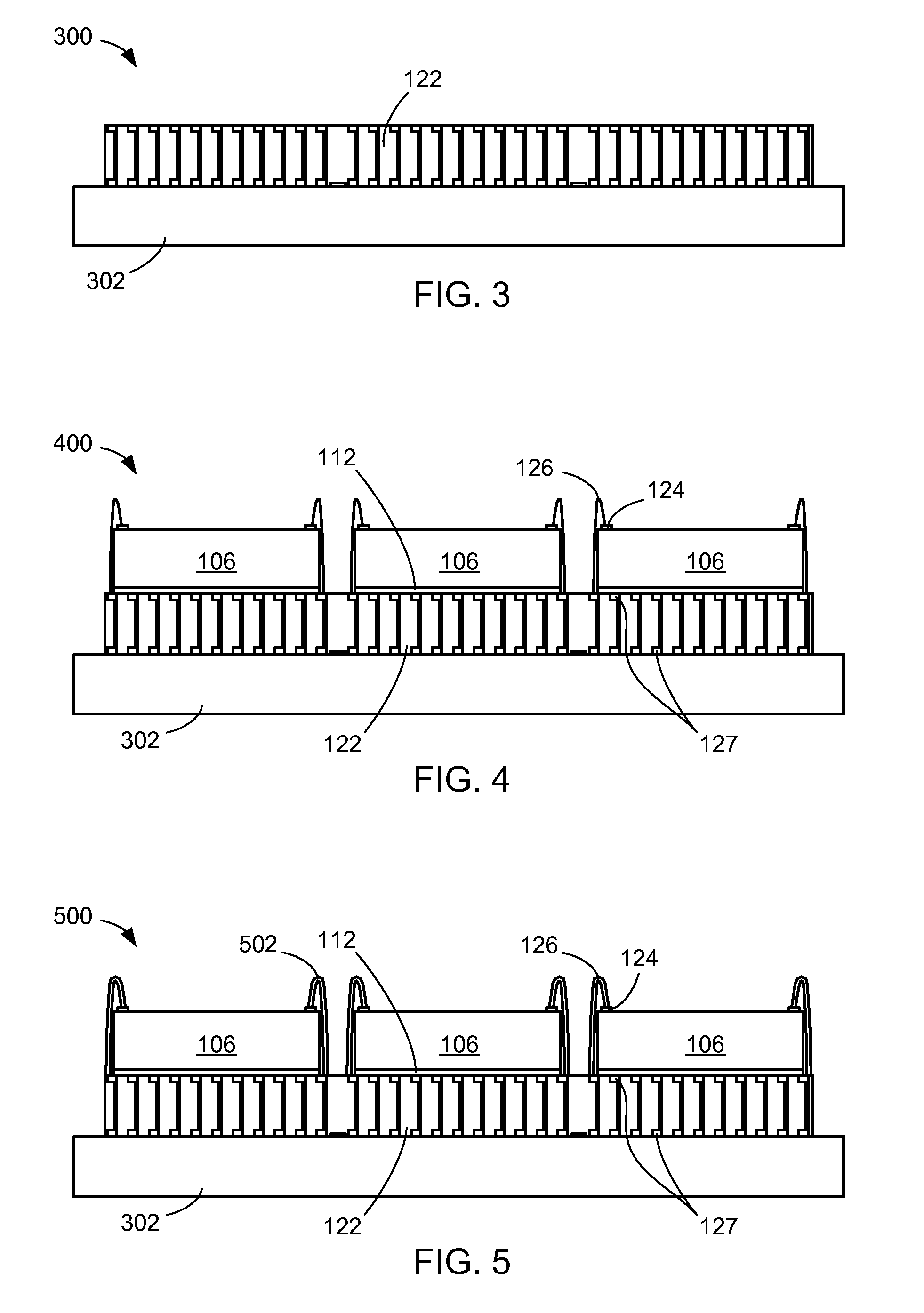
[0054]Referring now to FIG. 3, therein is shown a cross-sectional view similar to FIG. 1 of an unfinished semiconductor package 300 of the first embodiment of the present invention after a first intermediate stage of the process. The through silicon via interposer 122 is attached to a bottom carrier 302.

[0055]The bottom carrier 302 is typically made out of plastic tape material and could typically be stretched or extended horizontally.

[0056]Referring now to FIG. 4, therein is shown a cross-sectional view similar to FIG. 1 of an unfinished semiconductor pa...

second embodiment

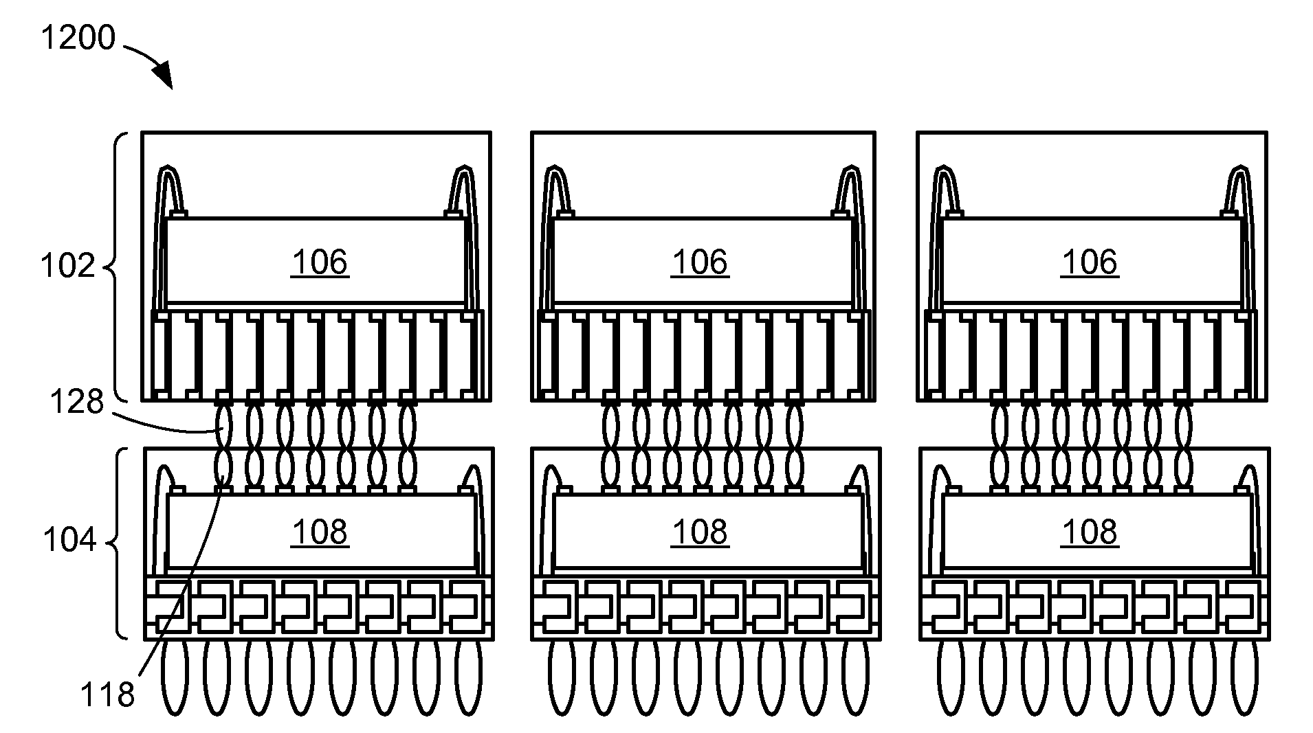
[0079]Referring now to FIG. 23, therein is shown a cross-sectional view similar to FIG. 1 of a semiconductor package of the present invention after a stage of singulation. A finished semiconductor package 2300 is shown. The finished semiconductor package 2300 is a Package-on-Package package (PoP). The finished semiconductor package 2300 has the top package 102 and the bottom package 104. The top semiconductor die 106 is embedded in the top package 102. The bottom semiconductor die 108 is embedded in the bottom package 104.

[0080]The bottom semiconductor die 108 is attached to the substrate interposer 110 through the die paste layer 112. The substrate interposer may be a laminated substrate. The bottom bonding pad 114 is shown on the bottom semiconductor die 108. The bottom bonding pad 114 is present on both the active center face as well as the periphery of the bottom semiconductor die 108. One bottom bonding pad 114 is attached to one end of the bottom bonding wire 116. The other en...

third embodiment

[0091]Referring now to FIG. 24, therein is shown a cross-sectional view similar to FIG. 1 of a semiconductor package of the present invention after a stage of singulation. A finished semiconductor package 2400 is shown. The finished semiconductor package 2400 is a Package-on-Package package (PoP). The finished semiconductor package 2400 has the top package 102 and the bottom package 104. A top semiconductor flip chip die 2406 is embedded in the top package 102. The bottom semiconductor die 108 is embedded in the bottom package 104.

[0092]The bottom semiconductor die 108 is attached to the substrate interposer 110 through the die paste layer 112. The substrate interposer may be a laminated substrate. The bottom bonding pad 114 is shown on the bottom semiconductor die 108. The bottom bonding pad 114 is present on both the active center face as well as the periphery of the bottom semiconductor die 108. One bottom bonding pad 114 is attached to one end of the bottom bonding wire 116. The...


PUM


Abstract

A semiconductor package system includes: providing a top package, a through silicon via interposer embedded in the top package; providing a bottom package having a bottom semiconductor die with a top connection adjacent the center active face thereof, a substrate interposer being embedded in the bottom package, the bottom semiconductor die being attached to the substrate interposer; and attaching the top package to the bottom package, the top package having the through silicon via interposer having a via connected to the top connection.

Description

TECHNICAL FIELD[0001]The present invention relates generally to semiconductor packages, and more particularly to a system for a semiconductor package for a smaller and thinner stacked solution.BACKGROUND ART[0002]In the electronics industry, the tendency has been to reduce the size of electronic devices such as camcorders and portable telephones while increasing performance and speed. Integrated circuit packages for complex systems typically are comprised of multiple interconnected integrated circuit chips. The integrated circuit chips usually are made from a semiconductor material such as silicon or gallium arsenide. The integrated circuit chips may be mounted in packages that are then mounted on printed wiring boards.[0003]Typically, the packages on which these integrated semiconductor chips are mounted include a substrate or other chip-mounting device. Substrates are parts that provide the package with mechanical base support and a form of electrical interface that would allow th...

Claims


Application Information

Patent Timeline
Patent Type & Authority Applications(United States)
IPC IPC(8): H01L23/488H01L21/60
CPCH01L21/6835H01L2924/10253H01L23/49827H01L24/29H01L24/48H01L24/73H01L24/91H01L24/97H01L25/105H01L2221/68331H01L2221/68359H01L2224/16H01L2224/48091H01L2224/48227H01L2224/49171H01L2224/49175H01L2224/73207H01L2224/73265H01L2224/97H01L2924/01074H01L2924/01082H01L2924/14H01L2924/1433H01L2924/15311H01L2924/15331H01L2924/19107H01L23/147H01L2225/1058H01L2225/1023H01L23/3135H01L23/3121H01L24/49H01L2224/32225H01L2924/00014H01L2224/85H01L2924/00H01L2924/00012H01L2224/05573H01L2224/13025H01L2224/05568H01L2224/056H01L2924/181H01L2224/04042H01L2224/0554H01L2224/45099H01L2224/45015H01L2924/207H01L2224/05599H01L2224/0555H01L2224/0556
Inventor CHOI, DAESIKYANG, DEOKKYUNGKIM, SEUNG WON
Owner STATS CHIPPAC LTD
Why Eureka
Try Eureka