Circuit simulation based on gate spacing from adjacent MOS transistors

a technology of mos transistor and gate spacing, which is applied in the field of circuit simulation apparatus, can solve problems such as the threshold voltage of mos transistor, and achieve the effect of accurate estimation of the effect of gate spacing and improving the accuracy of circuit simulation

Inactive Publication Date: 2010-04-01
RENESAS ELECTRONICS CORP
View PDF7 Cites 5 Cited by
  • Summary
  • Abstract
  • Description
  • Claims
  • Application Information

AI Technical Summary

Benefits of technology

[0018]The present invention allows accurately estimating the effect of the gate spacing between adjacent

Problems solved by technology

First, the gate spacing from the adjacent transistor influences the impurity profile in the source and drain, and therefore influences the threshold voltage of the MOS transistor.
Second, the gate spacing from the adjacent transistor influences the actual width of

Method used


Image

  • Circuit simulation based on gate spacing from adjacent MOS transistors
  • Circuit simulation based on gate spacing from adjacent MOS transistors
  • Circuit simulation based on gate spacing from adjacent MOS transistors

Examples


Embodiment Construction

[0041]The invention will be now described herein with reference to illustrative embodiments. Those skilled in the art will recognize that many alternative embodiments can be accomplished using the teachings of the present invention and that the invention is not limited to the embodiments illustrated for explanatory purposes.

1. Concept of Circuit simulation technique

[0042]First, a description is given of the concept of a circuit simulation technique in one embodiment of the present invention, referring to FIG. 1.

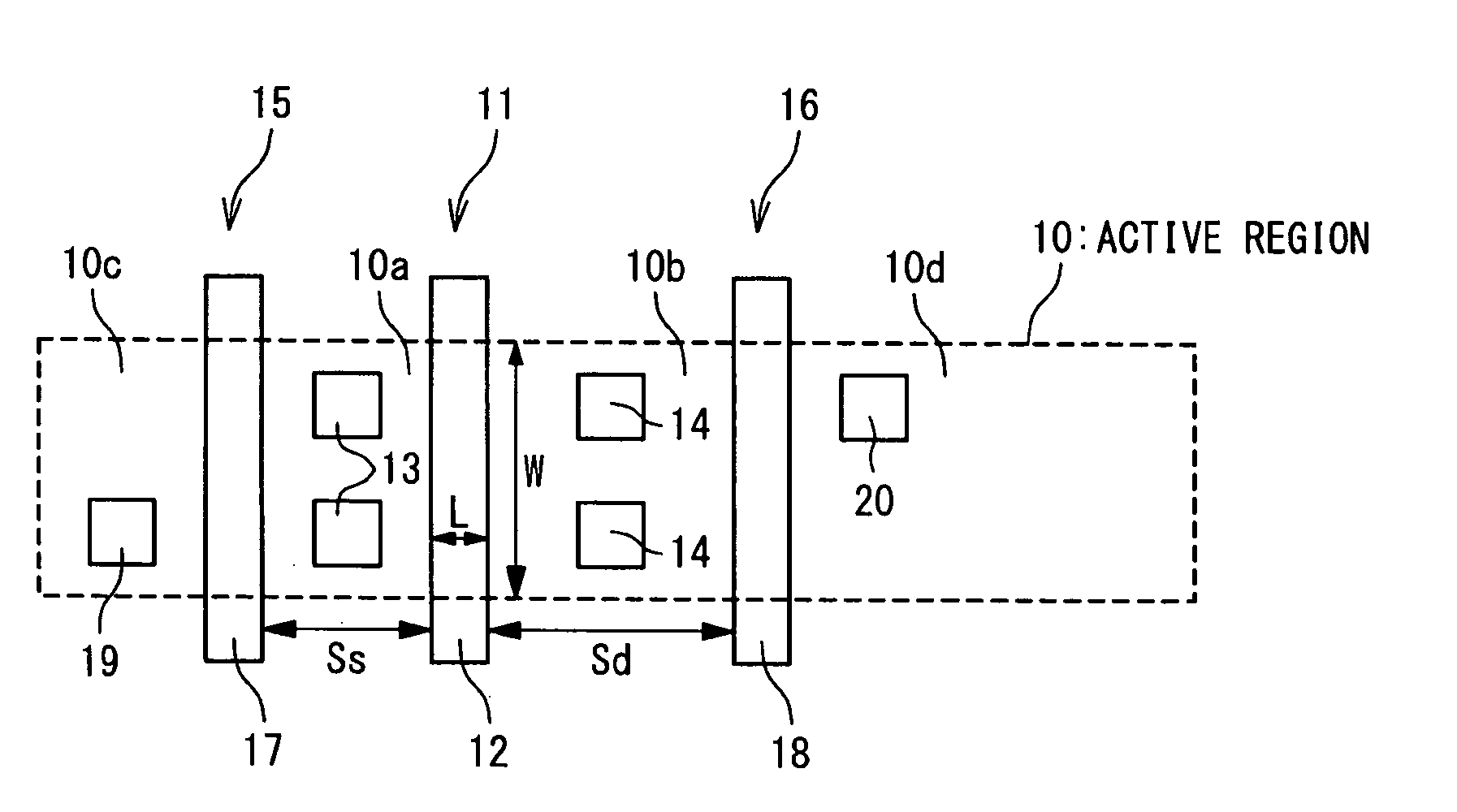
[0043]FIG. 1 is a diagram showing an example of the layout of an integrated circuit to be simulated. In FIG. 1, the reference numeral 10 denotes an active region and the reference numeral 11 denotes a MOS transistor to be simulated (hereinafter referred to as the “target transistor”). The reference numeral 12 denotes the gate of the MOS transistor 11. The gate 12 is provided so as to cross the active region 10. The region located immediately below the gate 12 in the active re...


PUM


Abstract

A circuit simulation apparatus is provided with a parameter calculating tool and a circuit simulator. The parameter calculating tool is configured to extract gate spacings between gates of a target MOS transistor and adjacent MOS transistors integrated in an integrated circuit from layout data of the integrated circuit, and to calculate a transistor model parameter corresponding to a threshold voltage of the target MOS transistor based on the extracted gate spacings. The circuit simulator is configured to perform circuit simulation of the integrated circuit by using the calculated transistor model parameter.

Description

INCORPORATION BY REFERENCE[0001]This application claims the benefit of priority based on Japanese Patent Application No. 2008-247920, filed on Sep. 26, 2008, the disclosure of which is incorporated herein by reference.BACKGROUND OF THE INVENTION[0002]1. Field of the Invention[0003]The present invention relates to a circuit simulation apparatus and a circuit simulation method, in particular, a technique for performing circuit simulation in consideration of variations in transistor characteristics depending on the shape of the peripheral pattern of the target transistor.[0004]2. Description of the Related Art[0005]One prominent property of high-integration LSI transistors is that the transistor characteristics thereof vary depending on the peripheral pattern shape. The magnitude of applied stress, the implantation dose of impurities and actual finished dimensions of a particular transistor are influenced by the peripheral pattern shape of the particular transistor. Such pattern depend...

Claims


Application Information

Patent Timeline
IPC IPC(8): G06F17/50G06F17/10
CPCG06F17/5036G06F30/367
Inventor SAKAMOTO, HIDEO
Owner RENESAS ELECTRONICS CORP
Why Eureka
Try Eureka