
Memory controller, nonvolatile storage device, nonvolatile storage system, and data writing method

a memory controller and storage device technology, applied in the field of memory controllers, can solve problems such as the change of data stored in other pages, and achieve the effect of high reliability

Inactive Publication Date: 2010-04-01
PANASONIC CORP
View PDF3 Cites 27 Cited by
  • Summary
  • Abstract
  • Description
  • Claims
  • Application Information

AI Technical Summary

Benefits of technology

"The present invention relates to a nonvolatile storage device that includes a rewritable nonvolatile memory, and a memory controller for controlling data writing and reading. The invention addresses the problem of writing error in a multi-level NAND flash memory that can affect data stored in an already written page. The invention provides a solution for writing data to the memory cells in a way that reduces the impact of errors and ensures the data is retained even if there are sudden power-shutdown or other disturbaning events."

Problems solved by technology

However, when one memory cell is configured striding over 2 pages, there is a problem that, if an error occurs during writing to one page, data stored in the other page change.

Method used


Image

  • Memory controller, nonvolatile storage device, nonvolatile storage system, and data writing method
  • Memory controller, nonvolatile storage device, nonvolatile storage system, and data writing method
  • Memory controller, nonvolatile storage device, nonvolatile storage system, and data writing method

Examples


first embodiment

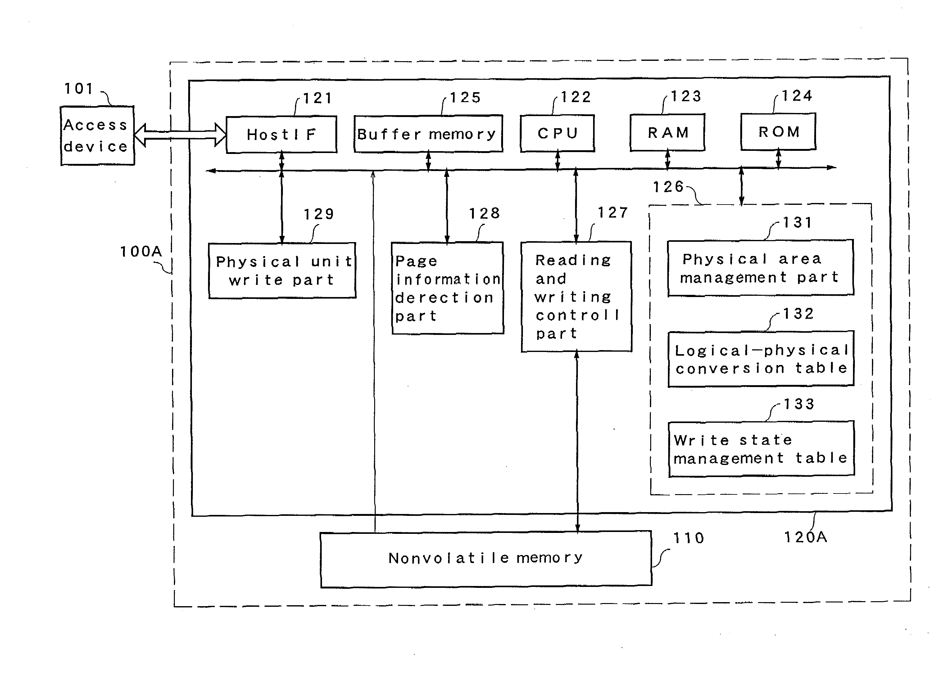
[0065]A nonvolatile storage system according to the first embodiment of the present invention will be described below. FIG. 7 is a block diagram of the nonvolatile storage system. The nonvolatile storage system is configured with a nonvolatile storage device 100A and an access device 101.

[0066]The nonvolatile storage device 100A includes a nonvolatile memory being composed of a flash memory and a memory controller 120A. The nonvolatile memory 110 is a multi-level NAND flash memory in which one memory cell retains data striding over two pages. For example, as shown in FIG. 8, the nonvolatile memory 110 consists of 4096 physical blocks of PB0 to PB4095. The physical block is a unit of erasing and each of the physical blocks consists of 128 pages. Each page is a unit of access from the memory controller 120A and has a storage capacity of 2112 bytes. Here, the nonvolatile memory is a memory having the same group configuration as FIG. 1.

[0067]The access device 101 orders reading and writ...

second embodiment

[0097]Next, a second embodiment of the present invention will be described. Since configuration of blocks showing configuration of a nonvolatile system according to the second embodiment is the same as that of FIG. 1, description for the configuration of blocks is omitted.

[0098]A multi-level nonvolatile memory as shown in FIG. 3 also exists other than the multi-level nonvolatile memory in which a page group is completed by being closed in units of two pages or four pages as shown in FIG. 1 and FIG. 2. In this nonvolatile memory shown in FIG. 3, since the physical unit of a model in the first embodiment is not closed in a specific unit, application of the nonvolatile storage system according to the first embodiment cannot be realized. Even in such a case, in order to prevent data destruction by data writing, a concept of a physical unit is extended in the second embodiment.

[0099]Next, writing process according to the second embodiment will be described by using a flowchart of writing...


PUM


Abstract

Used is a nonvolatile memory such as a multi-level NAND flash memory having memory cells for holding data of a plurality of pages. When the data is to be written in the nonvolatile memory 110, a physical unit is consisted in units of a plurality of paired pages. When all the physical units cannot be written, the data is copied from an old physical block holding an already written effective data, and is written in a new physical block till the written, from the first section of a new physical unit, so that an error can be prevented.

Description

TECHNICAL FIELD[0001]The present invention relates to a nonvolatile storage device including a rewritable nonvolatile memory, and a memory controller, a nonvolatile storage system, and a data writing method for controlling this device.BACKGROUND ART[0002]A nonvolatile storage device including a rewritable nonvolatile main memory is widely demanded mainly in a semiconductor memory card. The memory card includes a flash memory as a nonvolatile memory and includes a memory controller for controlling it. The memory controller controls reading and writing data to the flash memory in accordance with directions of reading and writing from an access device such as a digital still camera and personal computer (PC) body.[0003]In a nonvolatile storage device employing a nonvolatile memory, a device that rewrites data in a way of additionally writing is known (Patent document 1). In this nonvolatile storage device, when write data from a host are smaller than units of an erase block, the writin...

Claims


Application Information

Patent Timeline
Patent Type & Authority Applications(United States)
IPC IPC(8): G06F12/00G06F12/08
CPCG06F12/0246
Inventor INOUE, MANABUNAKANICHI, MASAHIROIZUMI, TOMOAKIMORI, HIRONORIMAKI, KUNIHIROHONDA, TOSHIYUKI
Owner PANASONIC CORP
Learn More