

Scanning optical device and image forming apparatus using the same
- Summary
- Abstract
- Description
- Claims
- Application Information
AI Technical Summary
Benefits of technology
Problems solved by technology
Method used
Image

Examples
embodiment 1
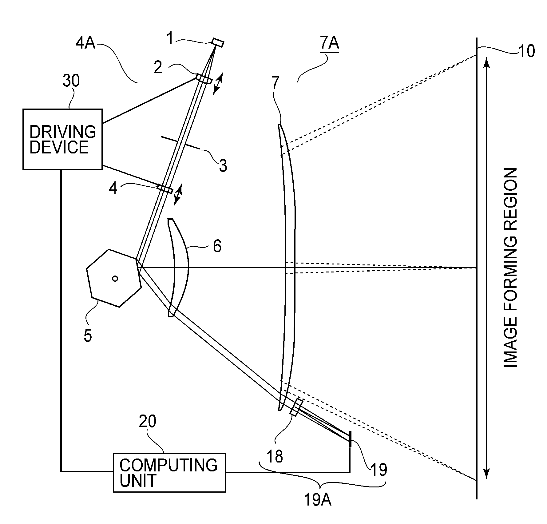
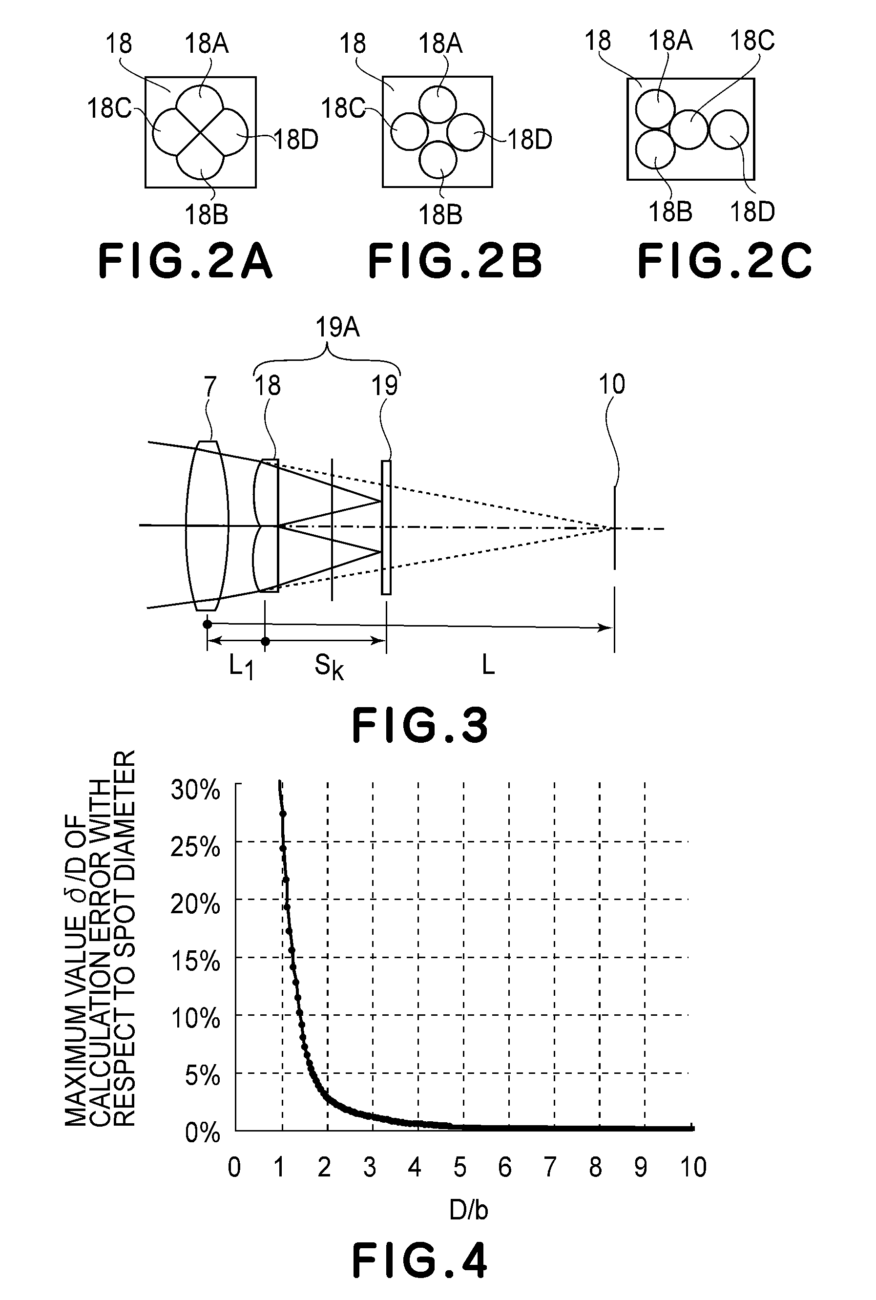
[0059]FIG. 1 through FIG. 8 are schematic diagrams of a first embodiment of the present invention. Of these drawings, FIG. 1 is a schematic diagram in the main-scan section of the first embodiment of the present invention. FIGS. 2A-2C are schematic diagrams each illustrating the shape of pupil dividing means of FIG. 1.
[0060]FIG. 3 is a schematic diagram illustrating the positional relationship of a third optical system 18 comprised of pupil dividing means which is disposed after an optical element 7 of a second optical system of FIG. 1 which is closest to the scan surface. FIG. 4 is a graph showing the relationship of the ratio of a spot diameter to the sensor pitch and a calculation error of the correlation calculation made by an arithmetic unit 20.
[0061]FIG. 5 is a schematic diagram illustrating the light path and parameters in the in-focus state and the focal shift state. FIG. 6 is a diagram showing signal waveforms at a photodetecting device, in the in-focus state and the focal ...
embodiment 2
[0153]FIG. 16 through FIG. 18 are schematic diagrams of a second embodiment of the present invention.
[0154]FIG. 16 is a schematic diagram in the main-scan section of the second embodiment of the present invention. FIGS. 17A-17C are schematic diagrams each illustrating the shape of the pupil dividing means of FIG. 16. FIG. 18 illustrates a modified form of the second embodiment.
[0155]In these drawings, denoted at 1 is light source means which comprises a semiconductor laser, for example. Denoted at 2 is a condenser lens (collimator lens) which serves to convert a light beam emitted from the light source means 1 into an approximately parallel light beam (or a divergent light beam or a convergent light beam). Denoted at 3 is an aperture stop which functions to shape the light beam from the condenser lens 2 into an optimum beam profile. Denoted at 4 is a cylindrical lens which has a finite power (refracting power) only in the sub-scan direction (sub-scan section).
[0156]The condenser len...
embodiment 3
[0177]FIG. 19 through FIG. 21 are schematic diagrams of a third embodiment of the present invention.
[0178]FIG. 19 is a schematic diagram in the main-scan section of the third embodiment of the present invention. FIG. 20 is a schematic diagram illustrating the positional relationship of a detecting system 19A in an example wherein pupil dividing means 38 is disposed before (deflecting means 5 side of) an optical element 7 of a second optical system 7A which element is closest to the scan surface. FIG. 21 illustrates a modified form of the third embodiment.
[0179]In these drawings, denoted at 1 is light source means which comprises a semiconductor laser, for example. Denoted at 2 is a condenser lens (collimator lens) which serves to convert a light beam emitted from the light source means 1 into an approximately parallel light beam (or a divergent light beam or a convergent light beam). Denoted at 3 is an aperture stop which functions to shape the light beam from the condenser lens 2 i...
PUM
 Abstract
Description
Claims
Application Information