Packaging substrate

Inactive Publication Date: 2010-04-22
PHOENIX PRECISION TECH CORP
3 Cites 2 Cited by

AI-Extracted Technical Summary

Problems solved by technology

Hence, the strength of joints is insufficient to endure the stress between the chip and the substrate.
Therefore, the phenomenon of joint breakage will become more serious.
Furthermore, when the shapes of the openings of th...

Method used

[0030]In conclusion, the packaging substrate of the present invention can enhance the adhesive strength between metal bumps and a solder mask by dielectric rings formed with a photosensitive dielectric material, wherein the dielectric rings are formed between the metal bumps and the sold...

Benefits of technology

[0008]The object of the present invention is to provide a packaging substrate, which can improve the adhesive strength between metal bumps and a solder mask. He...

Abstract

A packaging substrate is disclosed, which comprises: a substrate body, wherein a surface thereof has a plurality of conductive pads and a solder mask disposed on the surface and having a plurality of openings to expose the conductive pads; dielectric rings disposed on the inner walls of the openings and extending to parts of the surface of the solder mask surrounding the openings; and metal bumps disposed in the openings and on the conductive pads exposed thereby, and combined with the dielectric rings.

Application Domain

Technology Topic

Image

  • Packaging substrate
  • Packaging substrate
  • Packaging substrate

Examples

  • Experimental program(1)

Example

[0020]Because of the specific embodiments illustrating the practice of the present invention, a person having ordinary skill in the art can easily understand other advantages and efficiency of the present invention through the content disclosed therein. The present invention can also be practiced or applied by other variant embodiments. Many other possible modifications and variations of any detail in the present specification based on different outlooks and applications can be made without departing from the spirit of the invention.
Embodiment for Manufacture
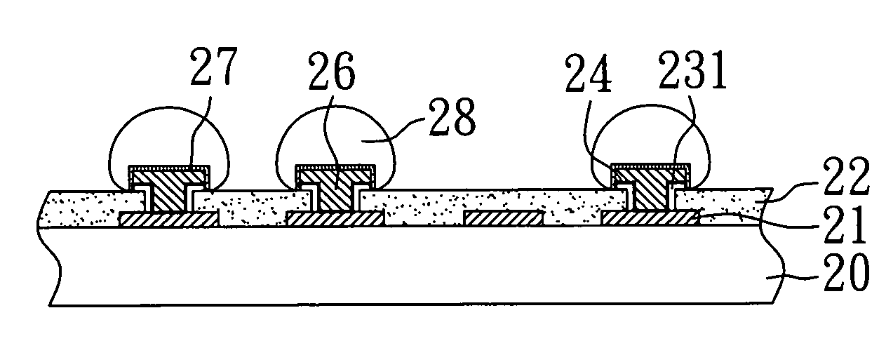
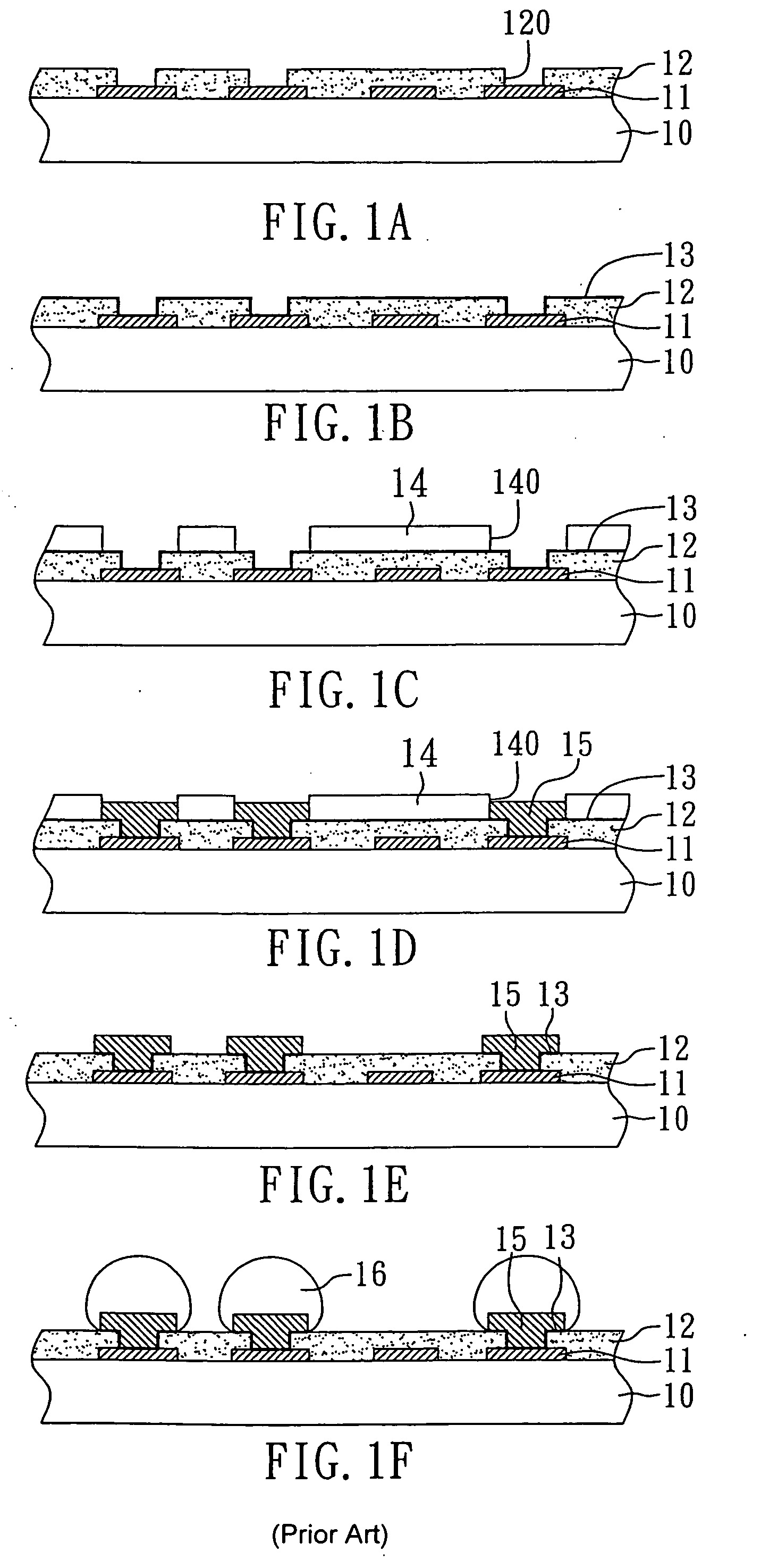
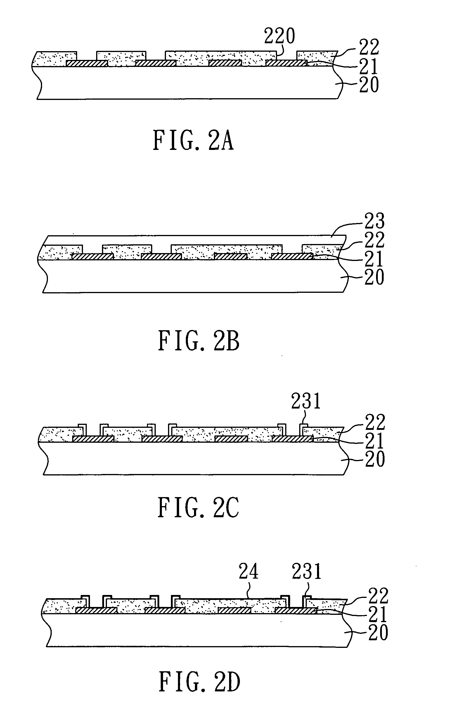
[0021]First, with reference to FIG. 2A, a substrate body 20 is provided, wherein a surface of the substrate body 20 has a plurality of conductive pads 21, and a solder mask 22 disposed on the surface and having a plurality of openings 220 to expose the conductive pads 21. Here, the material of the conductive pads 21 is selected from the group consisting of Cu, Sn, Ni, Cr, Ti, Cu/Cr alloy, and Sn/Pb alloy.
[0022]With reference to FIG. 2B, a photosensitive dielectric layer 23 is laminated on the surface of the substrate body 20, or the surface of the substrate body 20 is coated with a photosensitive dielectric layer 23. Then, with reference to FIG. 2C, dielectric rings 231 are formed on the inner walls of the openings 220, wherein the dielectric rings 231 extend to parts of the surface of the solder mask 22 surrounding the openings 220 through exposing and developing the photosensitive dielectric layer 23.
[0023]In the present embodiment, the material of the dielectric rings may be a photosensitive dielectric material, which can be selected from the group consisting of benzocylobuthene (BCB), Bismaleimide triazine (BT), Liquid Crystal Polymer, Poly-imide (PI), Poly(phenylene ether), Poly(tetra-fluoroethylene), Aramide, epoxy resin, and glass fiber.
[0024]With reference to FIG. 2D, a conductive seed layer 24 is formed on the surfaces of the solder mask 22, the dielectric rings 231, and the exposed parts of the conductive pads 21 by electroless plating.
[0025]Further, with reference to FIG. 2E, a resist layer 25 is formed on the surface of the conductive seed layer 24, and a plurality of resist-openings 250 are formed corresponding to the openings 220 of the solder mask 22. Herein, the resist layer 25 can be a dry film or a liquid photoresist film. In the present embodiment, the resist layer 25 is a dry film.
[0026]Then, with reference to FIG. 2F, metal bumps 26 are formed in the resist-openings 250 by electroplating. The material of the metal bumps 26 is selected from the group consisting of Cu, Ni, Cr, Ti, Cu/Cr alloy, and Sn/Pb alloy. In the present embodiment, the material of the metal bumps 26 is Cu. Finally, with reference to FIG. 2F, the resist layer 25, and the conductive seed layer 24 covered thereunder are removed.
[0027]In the aforementioned method, with reference to FIG. 2H, solder bumps 28 are further formed on the surfaces of the metal bumps 26. In addition, a metal adhesion layer 27 is further formed on the surface of the metal bumps 26 before the solder bump 28 is formed. Herein, the metal adhesion layer 27 is formed by physical deposition (such as sputtering or evaporation), or chemical deposition (such as electroless plating). Besides, the material of the metal adhesion layer 27 is selected from the group consisting of Sn, Ag, Ni, Au, Cr/Ti, Ni/Au, Ni/Pd, and Ni/Pd/Au. In the present embodiment, the material of the metal adhesion layer 27 is Sn.
Embodiment of Packaging Substrate
[0028]As shown in FIG. 2G, the present invention provides a packaging substrate, which comprises: a substrate body 20 wherein a surface thereof has a plurality of conductive pads 21, and a solder mask 22 disposed on the surface thereof and having a plurality of openings 220 to expose the conductive pads 21; dielectric rings 231 disposed on the inner walls of the openings 220, and extending to parts of the surface of the solder mask 22 surrounding the openings 20; and metal bumps 26 disposed in the openings 220 and on the conductive pads 21 exposed thereby, and combined with the dielectric rings 231.
[0029]With reference to FIG. 2H, the aforementioned packaging substrate further comprises solder bumps 28 formed on the surfaces of the metal bumps 26. In addition, the aforementioned packaging substrate further comprises a metal adhesion layer 27 formed between the metal bumps 26 and the solder bump 28. Herein, the material of the metal bumps 26 is selected from the group consisting of Cu, Ni, Cr, Ti, Cu/Cr alloy, and Sn/Pb alloy. In the present embodiment, the material of the metal bumps 26 is Cu. Besides, the material of the metal adhesion layer 27 is selected from the group consisting of Sn, Ag, Ni, Au, Cr/Ti, Ni/Au, Ni/Pd, and Ni/Pd/Au. In the present embodiment, the material of the metal adhesion layer 27 is Sn.
[0030]In conclusion, the packaging substrate of the present invention can enhance the adhesive strength between metal bumps and a solder mask by dielectric rings formed with a photosensitive dielectric material, wherein the dielectric rings are formed between the metal bumps and the solder mask. Hence, the problem of poor adhesive strength between the metal bumps and the solder mask in the prior art can be improved. Therefore, the packaging substrate of the present invention can conquer high stress imposed on joints between a packaging substrate and a semiconductor chip.
[0031]Although the present invention has been explained in relation to its preferred embodiment, it is to be understood that many other possible modifications and variations can be made without departing from the scope of the invention as hereinafter claimed.

PUM

no PUM

Description & Claims & Application Information

We can also present the details of the Description, Claims and Application information to help users get a comprehensive understanding of the technical details of the patent, such as background art, summary of invention, brief description of drawings, description of embodiments, and other original content. On the other hand, users can also determine the specific scope of protection of the technology through the list of claims; as well as understand the changes in the life cycle of the technology with the presentation of the patent timeline. Login to view more.

Similar technology patents

Lead frame

ActiveUS9653385B1Improve adhesive strengthSemiconductor/solid-state device detailsSolid-state devicesSilver oxideMoisture
Owner:SDI CORPORATION

Wafer processing base

ActiveUS20120202036A1Improve adhesive strengthImprove efficiencyFilm/foil adhesivesPolyureas/polyurethane adhesivesEngineeringResidual stress
Owner:LG CHEM LTD

Classification and recommendation of technical efficacy words

  • Improve adhesive strength

Capacitor and method of manufacturing the same

ActiveUS20170127521A1Improve adhesive strengthIncrease capacitance of capacitorFixed capacitor electrodesFinal product manufactureEngineeringCapacitor
Owner:SAMSUNG ELECTRO MECHANICS CO LTD

Lead frame

ActiveUS9653385B1Improve adhesive strengthSemiconductor/solid-state device detailsSolid-state devicesSilver oxideMoisture
Owner:SDI CORPORATION

Wafer processing base

ActiveUS20120202036A1Improve adhesive strengthImprove efficiencyFilm/foil adhesivesPolyureas/polyurethane adhesivesEngineeringResidual stress
Owner:LG CHEM LTD
Why Eureka
Try Eureka