
Wafer processing base

Active Publication Date: 2012-08-09
LG CHEM LTD
View PDF4 Cites 2 Cited by
  • Summary
  • Abstract
  • Description
  • Claims
  • Application Information

AI Technical Summary

Benefits of technology

[0018]When the toughness is less than 10 kg·mm, the substrate may become excessively stiff, or the photo-cured product may become difficult to form as a substrate. When the toughness is greater than 250 kg·mm, the cuttability may be reduced.
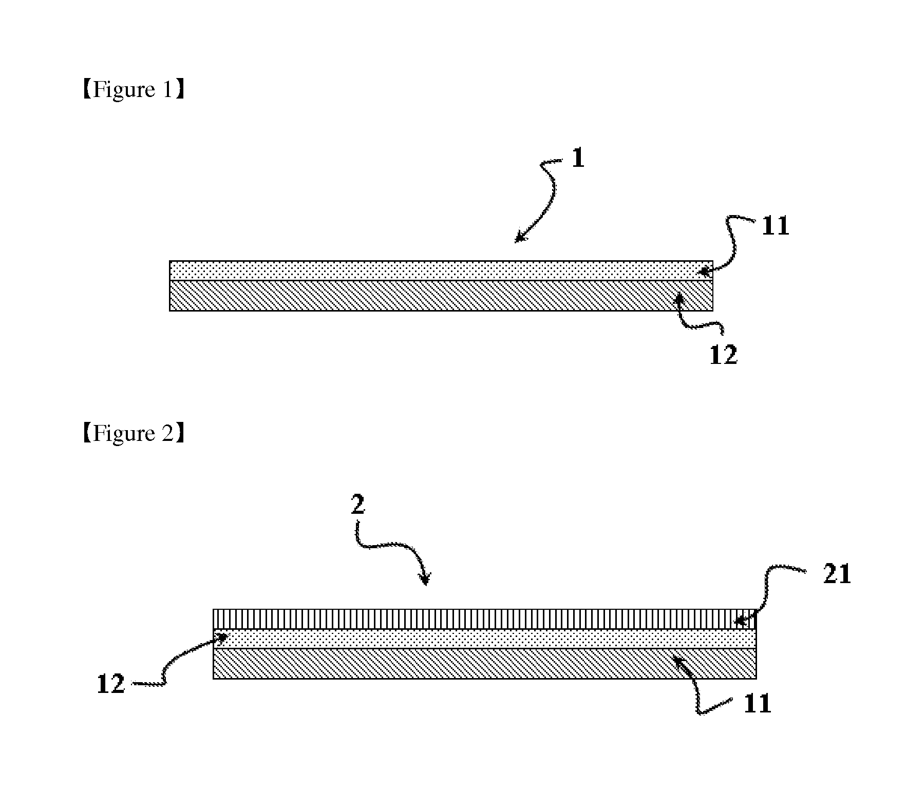
[0060]As shown in FIG. 2, a pressure-sensitive adhesive sheet 2 for processing a wafer may further include an appropriate releasing sheet 21 stacked on the pressure-sensitive adhesive layer 12 in order to prevent impurities from being introduced into the pressure-sensitive adhesive layer 12.

Problems solved by technology

However, when a hard substrate having a high melting point is used in order to secure heat resistance and dimensional stability, protection of the wafer is degraded and stress relaxation is also reduced, leading to a higher probability of damage to the wafer.
When the stress relaxation properties are reduced or a protrusion is present on the sheet, the wafer becomes easily damaged due to residual stress or due to non-uniform pressure.
When cuttability is decreased, a cutting defect may occur during the process, and thus wafer processing may be discontinuously performed.
Consequently, when the cuttability of the sheet for processing a wafer is decreased, production efficiency can be reduced and the wafer can be damaged.
However, there are no currently-known techniques, including Korean Patent Publication No. 2006-0047526, for a sheet for processing a wafer that satisfies all of the properties as described above.

Method used


Image

  • Wafer processing base
  • Wafer processing base

Examples


preparation example 1

Preparation of Partially Polymerized Product (A1)

[0067]A monomer mixture of 60 parts by weight of 2-ethylhexyl acrylate (2-EHA), 35 parts by weight of isobornyl acrylate (IBOA) and 5 parts by weight of acrylic acid (AA) was input into a 1 L reactor containing refluxed nitrogen gas and a cooling apparatus for easy control of the temperature. The nitrogen gas was then purged in order to remove oxygen. Afterwards, the mixture was homogenized while maintaining the temperature at 60° C., and the reaction was initiated by adding 0.015 parts by weight of diethylhexyl peroxydicarbonate as an initiator and 0.08 parts by weight of n-dodecyl mercaptan (n-DDM) as a chain transfer agent so as to prepare a partially-polymerized acrylic syrup having a solid content of 25 wt %, a weight average molecular weight of 400,000 and a glass transition temperature of −21° C. In the above, the weight average molecular weight of the syrup was the weight average molecular weight of the polymer included in the...

preparation example 2

Preparation of Partially Polymerized Product (A2)

[0068]A monomer mixture of 70 parts by weight of 2-ethylhexyl acrylate (2-EHA), 27 parts by weight of isobornyl acrylate (IBOA) and 3 parts by weight of hydroxyethyl acrylate (HEA) was input into a 1 L reactor containing refluxed nitrogen gas and a cooling apparatus for easy control of the temperature. The nitrogen gas was then purged in order to remove oxygen. Afterwards, the mixture was homogenized while maintaining the temperature at 60° C., and the reaction was initiated by adding 0.015 parts by weight of diethylhexyl peroxydicarbonate as an initiator and 0.04 parts by weight of n-dodecyl mercaptan (n-DDM) as a chain transfer agent so as to prepare a partially-polymerized acrylic syrup having a solid content of 35 wt %, a weight average molecular weight of 800,000 and a glass transition temperature of −36° C. In the above, the weight average molecular weight of the syrup was the weight average molecular weight of the polymer inclu...

example 1

[0069]A photo-curable composition was prepared by mixing 30 parts by weight of isobornyl acrylate (IBOA) with 70 parts by weight of the partially polymerized product (A1), adding 1.0 part by weight of 1,6-hexanediol diacrylate as a multi-functional acrylate and 1.0 part by weight of 1-hydroxycyclohexyl phenyl ketone (Igacure 184) as a photoinitiator thereto, and mixing and defoaming the resultant mixture. Afterwards, the resultant composition was coated on a polyester releasing film using a bar coater to a thickness of about 140 μm. Subsequently, to prevent the coated layer from being in contact with oxygen, another polyester releasing film was laminated on the coated layer while UV-A irradiation was performed using a metal halide lamp at a light intensity of 800 mJ / cm2, thereby preparing a photo-cured product (substrate).


PUM

PropertyMeasurementUnit
Temperatureaaaaaaaaaa

Abstract

Provided is a substrate for processing a wafer. The present invention can provide a substrate having excellent heat resistance and dimensional stability. The present invention can provide a substrate that has excellent stress relaxation properties, and therefore can prevent a wafer from being destroyed due to residual stress. Also, the present invention can provide a substrate that can prevent a wafer from being damaged or fried off due to a non-uniformly applied pressure during the wafer processing process, and that exhibits excellent cuttability. For these reasons, the substrate can be useful as a sheet for processing a wafer in various wafer preparation processes such as dicing, back-grinding, and picking-up.

Description

CROSS-REFERENCE TO RELATED APPLICATION[0001]This application is a continuation application (bypass application), under 35 USC §120, of International Patent Application No. PCT / KR2010 / 003827, filed on Jun. 15, 2010, which claims priority to and the benefit of Korean Patent Application No. 10-2009-0052945, filed Jun. 15, 2009, which is incorporated by reference in its entirety herein.BACKGROUND[0002]1. Field of the Invention[0003]The present invention relates to a substrate used for processing a wafer.[0004]2. Discussion of Related Art[0005]A preparation method for a semiconductor device that includes a back-grinding process or dicing process, during which a sheet such as a surface protective sheet or dicing sheet is used.[0006]Recently, since the demand for compact and lightweight semiconductor devices has increased, the performance of such a sheet for processing a wafer has accordingly become more and more important.[0007]For example, in order to make a circuit having a higher degre...

Claims


Application Information

Patent Timeline
IPC IPC(8): C08L33/08B29C35/08C09J7/24
CPCH01L21/6836H01L2221/6834H01L2221/68327C09J2203/326C09J2433/006C09J2463/006C09J2467/006C09J2471/006C09J2475/006C08G18/6229C08G18/8116C09J175/16C08G2170/40C08L33/08C09J7/24C09J2301/124C09J2301/416C09J2301/302C08F220/1808C08F220/1811C08F220/06C08F220/20
Inventor KIM, SE RAJOO, HYO SOOKCHANG, SUK KYSHIM, JUNG SUP
Owner LG CHEM LTD
Learn More