Light emitting diode, backlight assembly having the same and method thereof

a technology of light-emitting diodes and backlight assemblies, which is applied in the direction of instruments, discharge tubes, luminescent screens, etc., can solve the problems of inability to easily change the emission spectrum of these phosphors, limited number of conventional phosphors that have sufficient light conversion, and low spectra, etc., to achieve the effect of high efficiency and long-lasting of light-emitting diodes

Active Publication Date: 2010-04-29
SAMSUNG DISPLAY CO LTD
View PDF6 Cites 144 Cited by
  • Summary
  • Abstract
  • Description
  • Claims
  • Application Information

AI Technical Summary

Benefits of technology

[0010]The present invention provides a light emitting diode (LED) including a base, a light conversion layer and an LED chip. Some embodiments of the invention are capable of achieving high efficiency and long durability of the light emitting diode.

Problems solved by technology

However, there are a limited number of conventional phosphors that have sufficient light conversion efficiencies.
The emission spectrum of these phosphors is not easily changed.
Futhermore, the spectra are less than ideal in that the amount of light emitted varies as a function of wavelength.
Hence, even by combining several phosphors, an optimum white light source is not obtained.
Since ligands conjugated with the outer surface of the QD are organic substances, resin interacts with the ligands, thereby hampering efficiency and durability of QD phosphors.

Method used


Image

  • Light emitting diode, backlight assembly having the same and method thereof
  • Light emitting diode, backlight assembly having the same and method thereof
  • Light emitting diode, backlight assembly having the same and method thereof

Examples


Embodiment Construction

[0025]Hereinafter, the present invention will be described more fully with reference to the accompanying drawings, in which exemplary embodiments of the present invention are shown. This invention may, however, be embodied in many different forms and should not be construed as limited to the exemplary embodiments set forth herein. Rather, theses exemplary embodiments are provided so that this disclosure will be thorough and complete, and will fully convey the scope of the invention to those skilled in the art. Like reference numerals refer to like elements throughout.

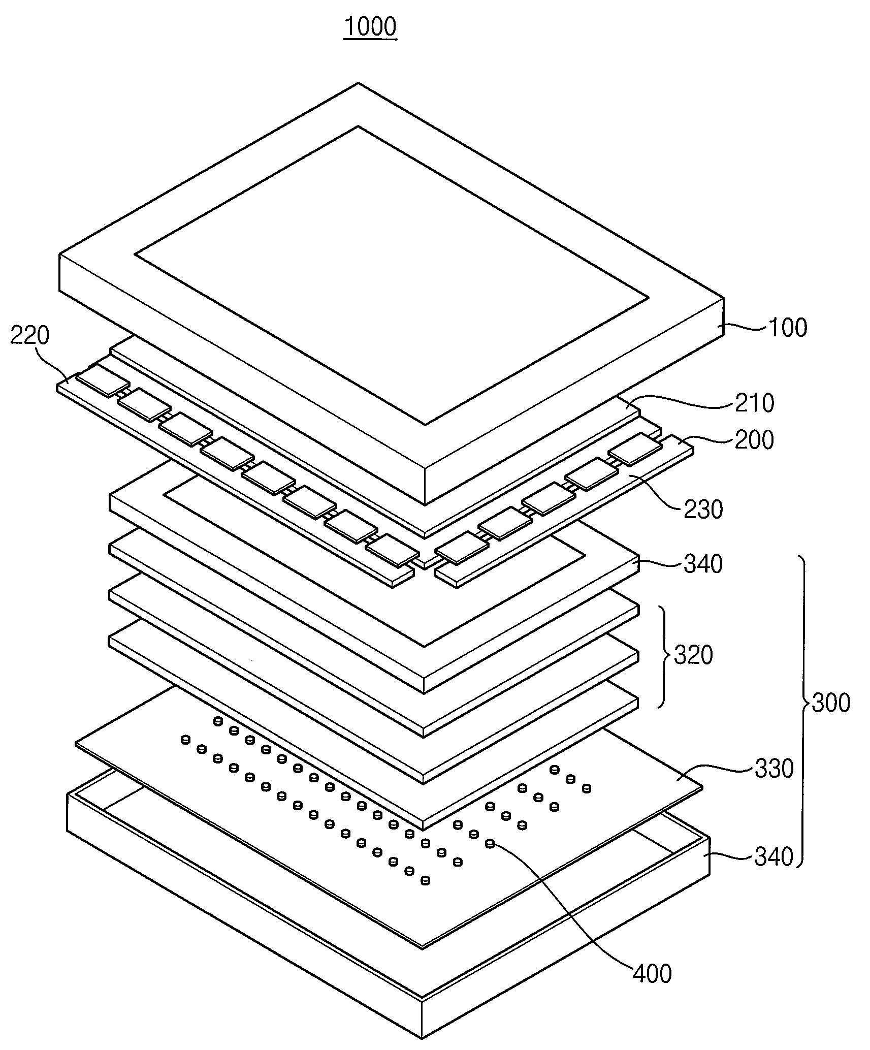
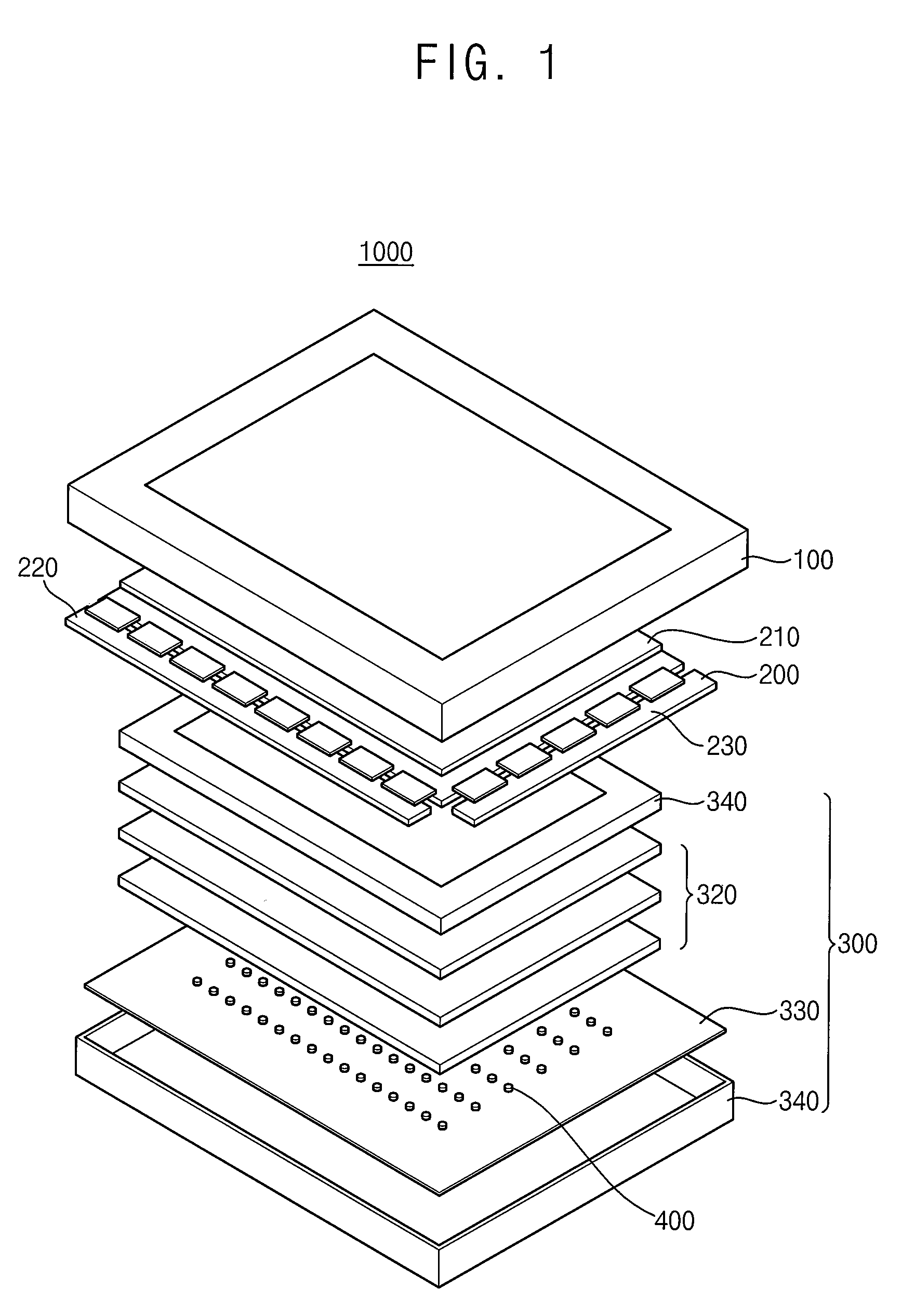
[0026]FIG. 1 is an exploded perspective view illustrating a first exemplary embodiment of a liquid crystal display 1000 according to the present invention. Referring to FIG. 1, a liquid crystal display may include a liquid crystal panel assembly 200, a backlight assembly 300, an upper receiving container 100, and a plurality of LEDs 400.

[0027]The liquid crystal panel assembly 200 may include a liquid crystal panel 210, ...


PUM


Abstract

A light emitting diode (LED). In one embodiment, the LED comprises a base including a cavity, an LED chip disposed on a bottom of the cavity and configured to generate a first light, and a light conversion layer. The light conversion layer includes an upper substrate, a lower substrate and a wavelength conversion particle. The light conversion layer is configured to convert a portion of the first light into a second light according to light emitted by the wavelength conversion particle. Furthermore, the light conversion layer is disposed on an upper surface of the base.

Description

PRIORITY STATEMENT[0001]This application claims priority under 35 U.S.C. §119 to Korean Patent Application No. 2008-105660, filed on Oct. 28, 2008 in the Korean Intellectual Property Office (KIPO), the contents of which are herein incorporated by reference in their entirety.BACKGROUND OF THE INVENTION[0002]1. Field of the Invention[0003]The present invention relates generally to light emitting diodes, and more particularly to light emitting diodes including a light conversion layer which converts received light to light with different wavelength.[0004]2. Description of the Related Art[0005]A white LED using a semiconductor, having advantages such as a long lifetime, capability of reduced size and operability at low voltage, is receiving attention as a next-generation LED.[0006]There has been proposed a conventional technique of realizing white light by applying red, green and blue phosphors around a UV short wavelength LED. In this configuration, the red, green and blue phosphors ar...

Claims


Application Information

Patent Timeline
Patent Type & Authority Applications(United States)
IPC IPC(8): G09F13/04H01L33/00H01L21/00
CPCG02F2001/133614H01L33/507H01L33/501G02F1/133614Y10S362/80
Inventor KIM, GUN-WOOPARK, JAE-BYUNGCHO, DON-CHANPARK, HAE-ILBYUN, JIN-SEOBSHIN, JUNG-HANYOON, SEON-TAEHONG, SUNG-JIN
Owner SAMSUNG DISPLAY CO LTD
Why Eureka
Try Eureka