Polarimetric imaging device optimized for polarization contrast

a polarimetric imaging and contrast technology, applied in the field of electromagnetic wave detectors, can solve the problem that the architecture described above still has a problem, and achieve the effect of not significantly affecting the contras

Inactive Publication Date: 2010-05-06
THALES SA
View PDF37 Cites 40 Cited by
  • Summary
  • Abstract
  • Description
  • Claims
  • Application Information

AI Technical Summary

Benefits of technology

[0018]This is why the present invention provides a novel polarimetric imaging device architecture having a matrix focal plane comprising a sensitive layer based on multiple quantum wells and optical coupling means for carrying out the polarimetric imaging without significantly impairing the contrast.

Problems solved by technology

The architecture described above nevertheless has a problem.

Method used


Image

  • Polarimetric imaging device optimized for polarization contrast
  • Polarimetric imaging device optimized for polarization contrast
  • Polarimetric imaging device optimized for polarization contrast

Examples


Embodiment Construction

First Example of an Imager According to the Invention

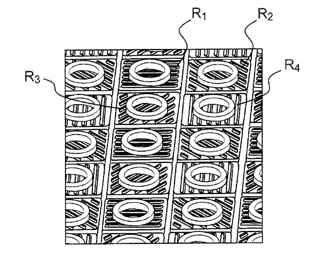
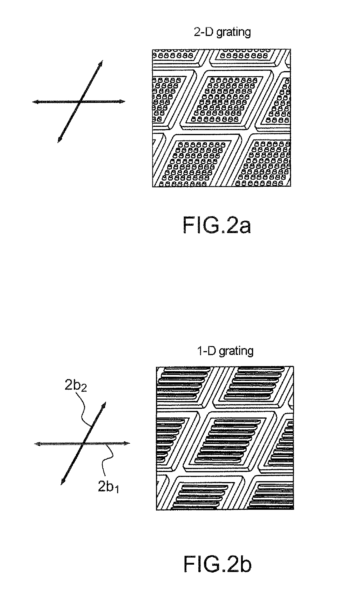
[0042]FIG. 4 illustrates a first example of the invention in which the imager comprises an MQW (multiple quantum well) structure comprising a set of detection elements at the surface of which selectively polarization-sensitive diffraction gratings have been produced. More precisely, this set of detection elements comprises subsets Eij consisting of four sub-pixels each respectively comprising a first 1-D diffraction grating sensitive to a first polarization RP1, a second 1-D diffraction grating sensitive to a second polarization RP2, a third 1-D diffraction grating sensitive to a third polarization RP3 and a fourth sub-pixel with no diffraction grating and referenced in the figure by R0. Typically, the second polarization is orthogonal to the first, the third polarization making an angle of about 45° to the first. Advantageously, the imager further includes signal processing means for recovering high-quality polarimetric imaging i...


PUM


Abstract

The invention relates to a polarimetric imaging device comprising a multiple-quantum-well structure operating on inter-sub-band transitions by absorbing radiation at a wavelength λ, said structure comprising a matrix of individual detection pixels, characterized in that the matrix is organized in subsets of four individual pixels, a first pixel comprising a first diffraction grating (RP1) sensitive to a first polarization, a second polarimetric pixel comprising a second diffraction grating (RP2) sensitive to a second polarization orthogonal to the first polarization, a third polarimetric pixel comprising a third diffraction grating (RP3) sensitive to a third polarization oriented at an angle between the first and second polarizations and a fourth pixel not comprising a polarization-selective diffraction rating (R2D).

Description

PRIORITY CLAIM[0001]This application claims priority to French Patent Application Number 08 05916, entitled Dispositif D'Imagerie Polarimetrique Optimise Par Rapport Au Contraste De Polarisation, filed on y Oct. 24, 2008.FIELD OF THE INVENTION[0002]The field of the invention is that of electromagnetic wave detectors made of a semiconductor and notably to wave detectors having a multiple-quantum-well structure, particularly those suitable for the infrared range.[0003]Rapid progress in epitaxial growth on GaAs-type substrates has resulted in the development of a new class of electromagnetic wave detectors using the absorption of radiation around a wavelength λ corresponding to the transition of electrons between various energy levels within the same energy band. The diagram in FIG. 1 illustrates this type of transition.BACKGROUND OF THE INVENTION[0004]Recent advances in the performance of such components are due in particular to the relatively easy fabrication of semiconductor multila...

Claims


Application Information

Patent Timeline
Patent Type & Authority Applications(United States)
IPC IPC(8): G01J4/00
CPCB82Y20/00H01L27/14621H01L27/14625H01L31/02327H01L31/035236H01L31/101H01L27/14649
Inventor NEDELCU, ALEXANDRUBOIS, PHILIPPECOSTARD, ERIC
Owner THALES SA
Why Eureka
Try Eureka