Conformal doping in p3i chamber

a technology of p3i chamber and doping chamber, which is applied in the direction of electrical discharge tubes, basic electric elements, electrical apparatus, etc., can solve the problems of adversely affecting the overall performance of electrical devices

Inactive Publication Date: 2010-05-06
APPLIED MATERIALS INC
View PDF13 Cites 7 Cited by
  • Summary
  • Abstract
  • Description
  • Claims
  • Application Information

AI Technical Summary

Benefits of technology

[0008]Methods for implanting ions into a substrate by a plasma immersion ion implantation process having a balanced etch-deposition process are provided. In one embodiment, a method for implanting ions into a substrate includes providing a substrate into a processing chamber, the substrate comprising substrate surface having one or more features formed therein and each feature having one or more horizontal surfaces and one or more vertical surfaces, generating a plasma from a gas mixture including a reacting gas adapted to produce ions, depositing a material layer on the substrate surface and on at least one horizontal surface of the substrate feature, implanting ions from the plasma into the substrate by an isotropic process into at least one horizontal surface and into at least one vertical surface, and etching the material layer on the substrate surface and the at least one horizontal surface by an anisotropic process.
[0009]In another embodiment, a method for implanting ions into a substrate includes providing a substrate into a processing chamber, the substrate comprising substrate surface having one or more features formed therein and each feature having one or more horizontal surfaces and one or more vertical surfaces, generating a plasma from a gas mixture including a reacting gas adapted to produce ions, depositing a material layer on the substrate surface and on at least one horizontal surface of the substrate feature, implanting ions from the plasma into the substrate by an isotropic process into at least one horizontal surface and at least one vertical surface, sputtering a portion of the material layer, a portion of the implanted ions, or combinations thereof, from the at least one horizontal surface to at least one vertical surface, and etching the substrate surface and the one or more horizontal surfaces and one or more vertical surfaces by an isotropic process.
[0010]In another embodiment, a method for implanting ions into a substrate includes providing a substrate into a processing chamber, the substrate comprising substrate surface having one or more features formed therein and each feature having one or more horizontal surfaces and one or more vertical surfaces, depositing a material layer on the substrate surface and on at least one horizontal surface of the substrate feature, generating a plasma from a gas mixture including a reacting gas adapted to produce ions, implanting ions from the plasma into the substrate by an isotropic process into at least one horizontal surface and into at least one vertical surface, and etching the material layer on the substrate surface and the at least one horizontal surface by an anisotropic process.

Problems solved by technology

Non-conformal ion doping may result in insufficient and / or non-uniform ion concentration, profile, dimension, and distribution across the substrate surface, especially in feature definitions formed in the substrate surface, thereby adversely affecting the overall electrical device performance.

Method used


Image

  • Conformal doping in p3i chamber
  • Conformal doping in p3i chamber
  • Conformal doping in p3i chamber

Examples


Embodiment Construction

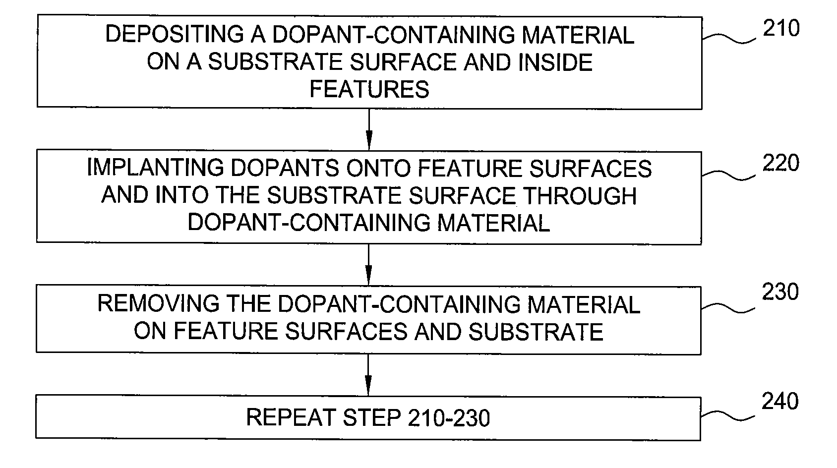
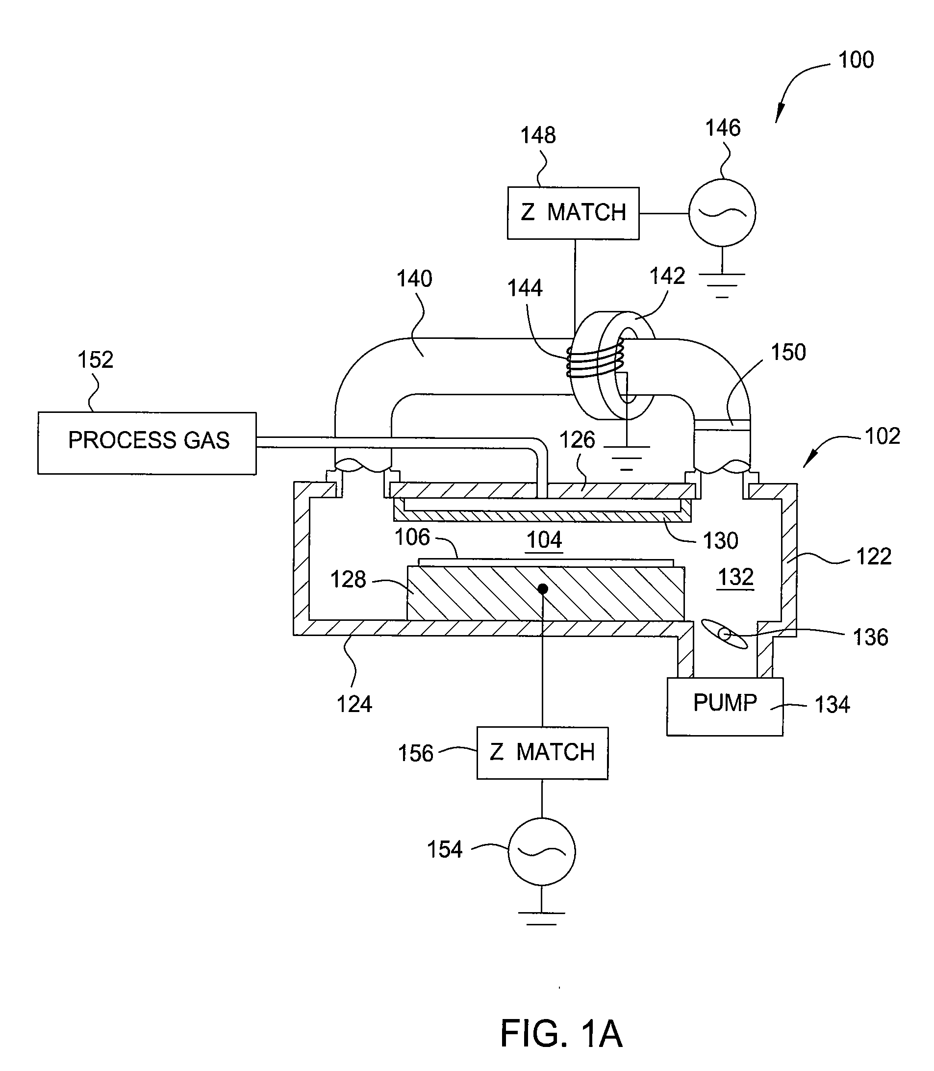
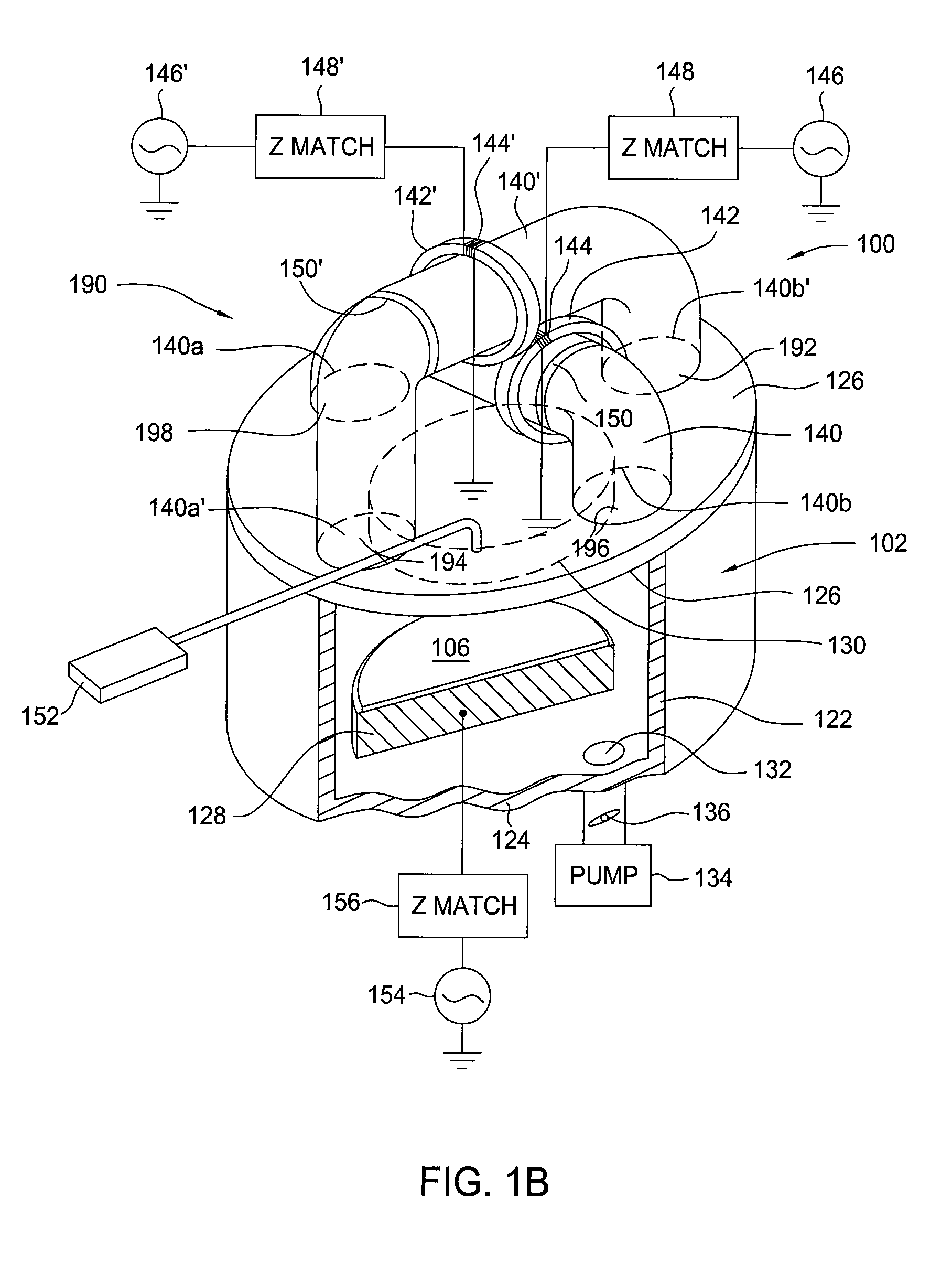
[0019]Embodiments of the invention provide methods for implanting ions into a substrate by a plasma immersion ion implantation process. The invention may be used in gate structure or source / drain region formation including, but not limited to, poly doping, counter-poly doping, ultra shallow junction, and conformal doping for structures formed on a substrate, among others. The ion implantation process may be utilized in different applications, such as DRAM, logic products, and flash memory. In one embodiment, the ion implantation process is performed by supplying a gas mixture including a reacting gas, for example a boron-containing gas. A plasma is generated to dissociate ions from the gas mixture, thereby forming a source of ions that are accelerated toward and implanted into an electrically biased substrate and / or deposited as a material layer on the substrate surface. The implanted ions may also be referred to as dopants. The deposited material may be partially or completely remo...


PUM


Abstract

Methods for implanting ions into a substrate by a plasma immersion ion implanting process are provided. In one embodiment, a method for implanting ions into a substrate includes providing a substrate into a processing chamber, the substrate comprising substrate surface having one or more features formed therein and each feature having one or more horizontal surfaces and one or more vertical surfaces, generating a plasma from a gas mixture including a reacting gas adapted to produce ions, depositing a material layer on the substrate surface and on at least one horizontal surface of the substrate feature, implanting ions from the plasma into the substrate by an isotropic process into at least one horizontal surface and into at least one vertical surface, and etching the material layer on the substrate surface and the at least one horizontal surface by an anisotropic process.

Description

CROSS-REFERENCE TO RELATED APPLICATIONS[0001]This application claims benefit of U.S. provisional patent application Ser. No. 61 / 110,475, filed Oct. 31, 2008, which is herein incorporated by reference.BACKGROUND OF THE INVENTION[0002]1. Field of the Invention[0003]Embodiments of the invention generally relate to the field of semiconductor manufacturing processes and devices, more particular, to methods of implanting ions into a substrate by a plasma immersion ion implantation process.[0004]2. Description of the Related Art[0005]Integrated circuits may include more than one million micro-electronic field effect transistors (e.g., complementary metal-oxide-semiconductor (CMOS) field effect transistors) that are formed on a substrate (e.g., semiconductor wafer) and cooperate to perform various functions within the circuit. A CMOS transistor comprises a gate structure disposed between source and drain regions that are formed in the substrate. The gate structure generally comprises a gate...

Claims


Application Information

Patent Timeline
Patent Type & Authority Applications(United States)
IPC IPC(8): H01L21/265H01L21/302H01L21/322
CPCH01J37/32412H01L21/2236H01L21/265
Inventor PORSHNEV, PETER I.SCOTNEY-CASTLE, MATTHEW D.FOAD, MAJEED A.
Owner APPLIED MATERIALS INC
Why Eureka
Try Eureka