Control apparatus for plasma immersion ion implantation of a dielectric substrate

a control apparatus and dielectric substrate technology, applied in the field of plasma processing systems, can solve the problems of difficult voltage coupling through the insulating substrate, limited voltage coupling, and limited voltage coupling

Inactive Publication Date: 2012-01-05
VARIAN SEMICON EQUIP ASSOC INC
View PDF16 Cites 36 Cited by
  • Summary
  • Abstract
  • Description
  • Claims
  • Application Information

AI Technical Summary

Benefits of technology

[0009]Exemplary embodiments of the present invention are directed to a control apparatus for plasma immersion ion implantation of a dielectric substrate and an associated method. In an exemplary embodiment, a plasma processing tool comprises a plasma chamber configured to generate a plasma having ions from a gas introduced into the chamber. A platen is configured to support and electrically connect to an insulator substrate for plasma doping. The platen is connected to a voltage source supplying negative bias voltage pulses at a first potential to the platen and to the

Problems solved by technology

Implantation using a PLAD tool is typically limited to conducting substrates or a semiconductive (e.g., Si) workpiece due to the ability to bias a conductive substrate to attract ions across the plasma sheath for implantation therein.
However, it is difficult to couple voltage through an insulating substrate in order to maintain the proper biasing of the substrate to attract the ions across the plasma sheath for implantation.
In particular, for relatively thick insulating substrates, voltage coupling is limit

Method used


Image

  • Control apparatus for plasma immersion ion implantation of a dielectric substrate
  • Control apparatus for plasma immersion ion implantation of a dielectric substrate
  • Control apparatus for plasma immersion ion implantation of a dielectric substrate

Examples


Embodiment Construction

[0019]The present invention will now be described more fully hereinafter with reference to the accompanying drawings, in which preferred embodiments of the invention are shown. This invention, however, may be embodied in many different forms and should not be construed as limited to the embodiments set forth herein. Rather, these embodiments are provided so that this disclosure will be thorough and complete, and will fully convey the scope of the invention to those skilled in the art. In the drawings, like numbers refer to like elements throughout.

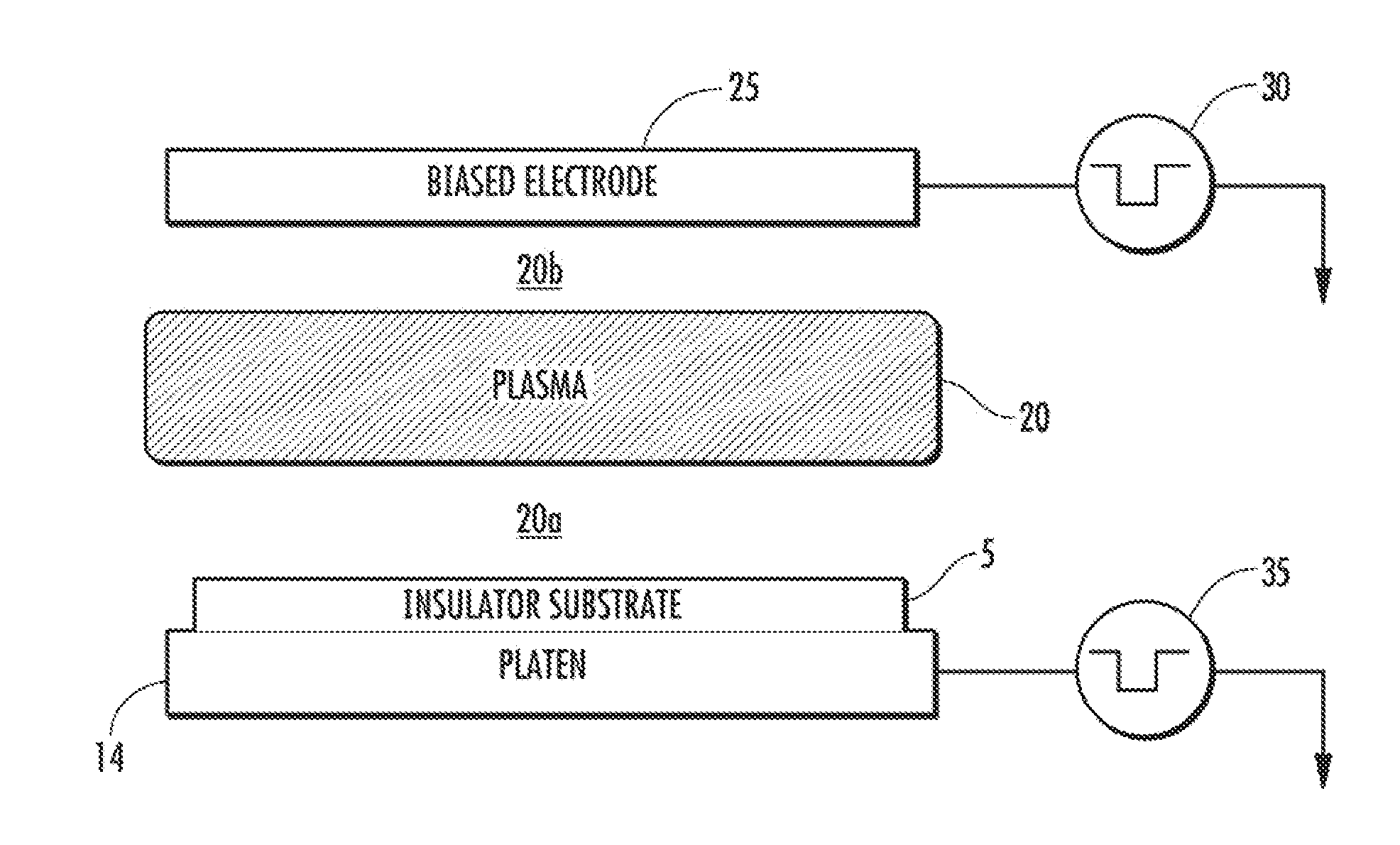
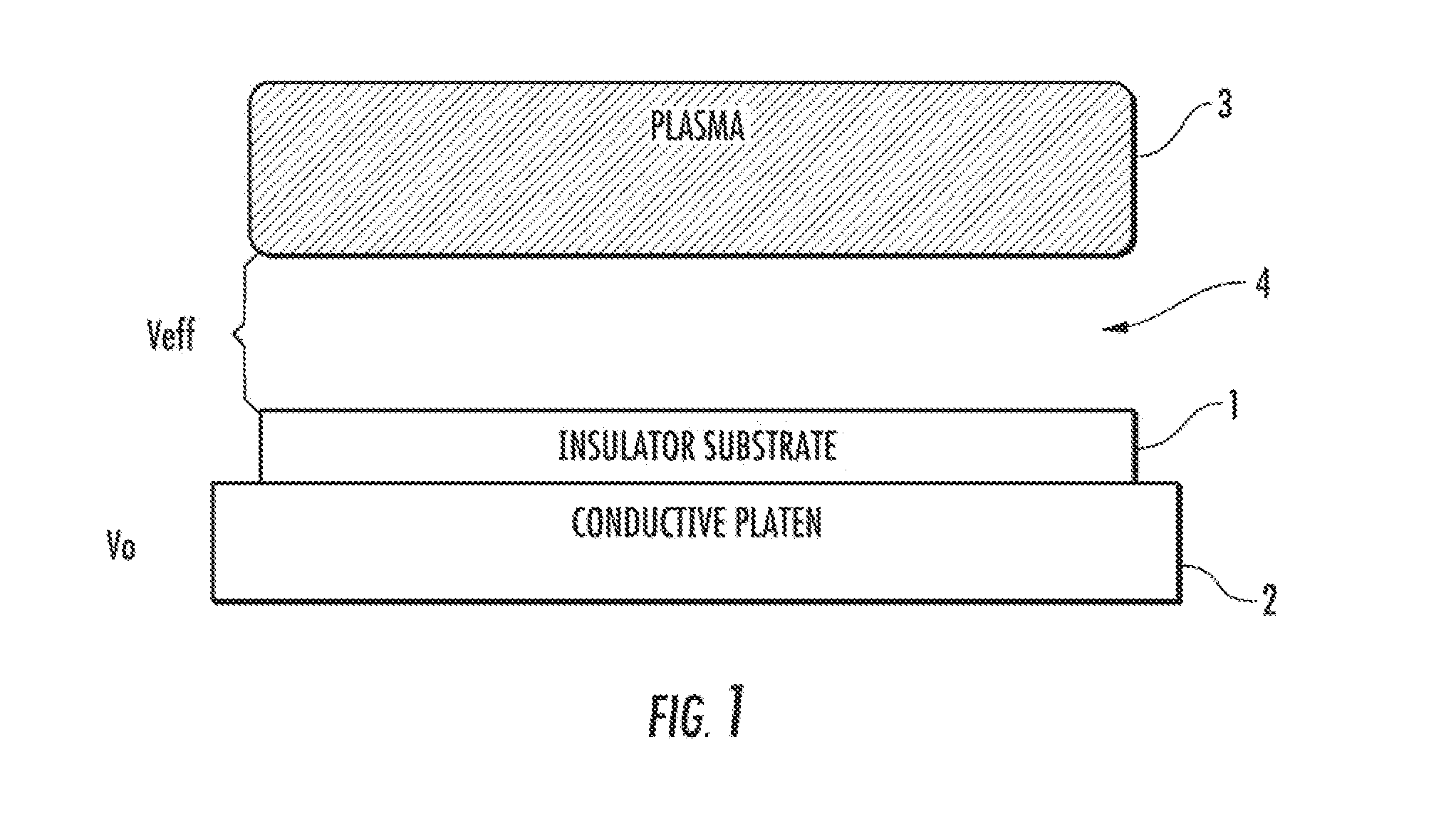
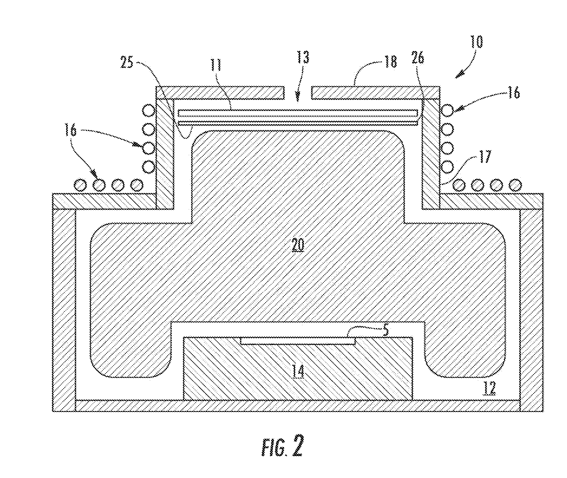
[0020]FIG. 2 is a schematic illustration of a simplified PLAD system or tool 10 in accordance with an exemplary embodiment of the present disclosure. The system 10 comprises a process chamber 12 having a pedestal or platen 14 to support an insulated target substrate 5. One or more reactive gases containing the desired dopant characteristics are fed into the process chamber 12 via a gas inlet 13 through a top plate 18 of the chamber. The re...


PUM

PropertyMeasurementUnit
Angleaaaaaaaaaa
Electric potential / voltageaaaaaaaaaa
Widthaaaaaaaaaa

Abstract

A control apparatus for plasma immersion ion implantation of a dielectric substrate which includes an electrode disposed above a generated plasma in a plasma chamber. The electrode is biased with negative voltage pulses at a potential that is higher than a potential of a substrate or cathode configured to receive ion implantation. The electrode is more negative to give the electrons generated as secondary electrons from the electrode sufficient energy to overcome the negative voltage of the high voltage sheath around the substrate thereby reaching the substrate. These electrons are accelerated toward the substrate to neutralize charge build-up on the substrate.

Description

BACKGROUND OF THE INVENTION[0001]1. Field of the Invention[0002]Embodiments of the invention relate to the field of plasma processing systems. More particularly, the present invention relates to an apparatus and method for improving and regulating voltage coupling for insulating target substrates used in plasma immersion ion implantation.[0003]2. Discussion of Related Art[0004]Plasmas are used in a variety of ways in semiconductor processing to implant wafers or substrates with various dopants, to deposit or to etch thin films. Such processes involve the directional deposition or doping of ions on or beneath the surface of a target substrate. Other processes include plasma etching, where the directionality of the etching species determines the quality of the trenches to be etched.[0005]Generally, plasma immersion ion implantation (PIII), also referred to as plasma doping (PLAD), implants dopants into a substrate. The plasma is generated by supplying energy to a neutral gas introduce...

Claims


Application Information

Patent Timeline
IPC IPC(8): C23C14/48C23C14/50C23C14/52H05F3/00
CPCC23C14/48H01J37/32935H01J37/32412C23C14/542H01J37/32
Inventor MILLER, TIMOTHYSINGH, VIKRAMGODET, LUDOLEAVITT, CHRISTOPHER J.
Owner VARIAN SEMICON EQUIP ASSOC INC
Why Eureka
Try Eureka