
Plasma immersion ion implantation process using an inductively coupled plasma source having low dissociation and low minimum plasma voltage

a plasma source and plasma technology, applied in the field of ion implantation using plasma immersion, can solve the problems of rapid thermal annealing by halogen lamps, loss of junction abruptness, and less efficiency of ion beam accelerators, and achieve the effect of higher ion flux

Inactive Publication Date: 2007-12-04
APPLIED MATERIALS INC
View PDF182 Cites 33 Cited by
  • Summary
  • Abstract
  • Description
  • Claims
  • Application Information

AI Technical Summary

Problems solved by technology

Such neutrals therefore impact the wafer at the original energy (e.g., 2 keV), so that they are implanted below the desired junction depth, due to the high energy tail, causing a loss of junction abruptness.
Moreover, rapid thermal annealing by halogen lamps, for example, tends to “wash out” the effect of the high energy tail due to diffusion.
However, as semiconductor circuit feature size decreases with progress in device speed, ion beam accelerators become less efficient.
However, dynamic surface annealing does not reduce the high energy tail.
Unfortunately, the lower ion energy in drift mode limits the ion beam flux (and current), so that the time required to reach the desired high dopant concentration can be as long as a half hour or one hour.
This problem arises particularly in shallow junction implant of light species such as Boron, in which the beam voltage must be reduced to avoid high velocity Boron ions being implanted below the desired junction depth.
The problem arises basically because the space charge effects in the ion beam produce repulsive forces between the ions in the beam in a radial direction, generally, limiting the beam density and therefore the beam current.
Such effects become more important as the beam energy is reduced (as it must be for implanting the lighter elements such as Boron), resulting in lower beam currents and longer implant times. Such long implant times greatly limit productivity and increase production costs.
In the future, feature sizes will decrease further, down to 45 nm, so that such problems will worsen in proportion as the technology advances.
These problems pertain particularly to cases in which the species to be implanted has a low atomic weight (such as Boron), so that the acceleration voltage must be small, which translates into a small ion beam flux and a long implant time.
However, while much of the implanted fluorine tends to diffuse out of the silicon crystal during annealing, a significant amount does not, leaving some crystal lattice sites that contain neither a semiconductor atom (Si) nor a dopant impurity atom (B), thus (for some applications) reducing the overall quality of the semiconductor material.
Therefore, this technique is not desirable universally for all applications.
Such advances in technology (where features size decreases to 65 nm and ultimately to 45 nm) render ion beam implantation of lighter dopants such as Boron impractical.
This is because the traditional ion beam implanter provides too little ion beam flux in such applications.
However, such plasma ion immersion implantation has been plagued by various difficulties.
Accordingly, such a reactor is unacceptably sensitive to changes in the condition of the chamber surfaces due, for example, to contamination of the chamber surfaces.
As a result, such a plasma ion immersion implantation reactor cannot maintain a target junction depth or abruptness, for example, and is plagued by contamination problems.
One problem inherent with D.C. voltage applied to the wafer support is that its pulse width must be such that the dopant ions (e.g., Boron) are accelerated across the plasma sheath near the wafer surface with sufficient energy to reach the desired junction depth below the surface, while the pulse width must be limited to avoid (discharge) any charge build-up on the wafer surface that would cause device damage (charging damage).
The limited pulse width is problematic in that the periodic decrease in ion energy can result in deposition on the semiconductor surface rather than implantation, the deposition accumulating in a new layer that can block implantation during the pulse on times. Another problem arises because ions must impact the wafer surface with at least a certain target energy in order to penetrate the surface up to a desirable depth (the as-implanted junction depth) and become substitutional below the surface and up to the desired annealed junction depth during the annealing process.
Unfortunately, due to resistive and capacitive charging effects (RC time constant) on dielectric films on the wafer that tend to accompany a D.C. discharge, the ions reach the target energy during only a fraction of each pulse period (e.g., during the first microsecond), so that there is an inherent inefficiency.
This problem cannot be solved by simply increasing the bias voltage, since this would increase the junction depth beyond the desired junction depth.
This type of reactor reduces the problems associated with plasma maintenance from secondary electrons, but still suffers from the problems associated with pulsed D.C. voltages on the wafer discussed immediately above.
While such a reactor has reduced sensitivity to chamber surface conditions as compared to reactors employing a pulsed DC bias, it is still quite sensitive.
Also, ion energy and flux cannot be independently selected with a single RF power source.
Ion flux may still be unacceptably low for high throughput applications with a single RF power source.
One problem is that the magnetic field gradient is non-uniform, so that the radial distribution of plasma ion energy is non-uniform, causing non-uniform junction depths across the wafer.
Another problem is the relatively high ion energy directed at the wafer, limiting the degree to which junction depths can be minimized.
The problem with such an approach is that the ion density and flux is at least proportionately decreased, thus reducing the productivity of the reactor.
A related problem is that, because the plasma ion density at the wafer surface is reduced by the increased source-to-wafer distance, the chamber pressure must be reduced in order to reduce recombination losses.
However, the additional magnetic field would increase magnetic flux at the wafer surface, increasing the risk of charge damage to semiconductor structures on the wafer.
In summary, plasma immersion ion implantation reactors have various limitations, depending upon the type of reactor: plasma reactors in which a pulsed D.C. voltage is applied to the wafer pedestal are too sensitive to chamber conditions and are inefficient; and plasma reactors with microwave ECR sources tend to produce non-uniform results.

Method used


Image

  • Plasma immersion ion implantation process using an inductively coupled plasma source having low dissociation and low minimum plasma voltage
  • Plasma immersion ion implantation process using an inductively coupled plasma source having low dissociation and low minimum plasma voltage
  • Plasma immersion ion implantation process using an inductively coupled plasma source having low dissociation and low minimum plasma voltage

Examples


working examples

[0299]A principal application of a PIII reactor is the formation of PN junctions in semiconductor crystals. FIGS. 109 and 110 illustrate different stages in the deposition of dopant impurities in the fabrication of a P-channel metal oxide semiconductor field effect transistor (MOSFET). Referring first to FIG. 109, a region 9960 of a semiconductor (e.g., silicon) wafer may be doped with an N-type conductivity impurity, such as arsenic or phosphorus, the region 9960 being labeled “n” in the drawing of FIG. 109 to denote its conductivity type. A very thin silicon dioxide layer 9962 is deposited on the surface of the wafer including over n-type region 9960. A polycrystalline silicon gate 9964 is formed over the thin oxide layer 9962 from a blanket polysilicon layer that has been doped with boron in the PIII reactor. After formation of the gate 9964, p-type dopant is implanted in the PIII reactor to form source and drain extensions 9972 and 9973. Spacer layers 9966 of a dielectric materi...


PUM

PropertyMeasurementUnit
bias frequencyaaaaaaaaaa

Abstract

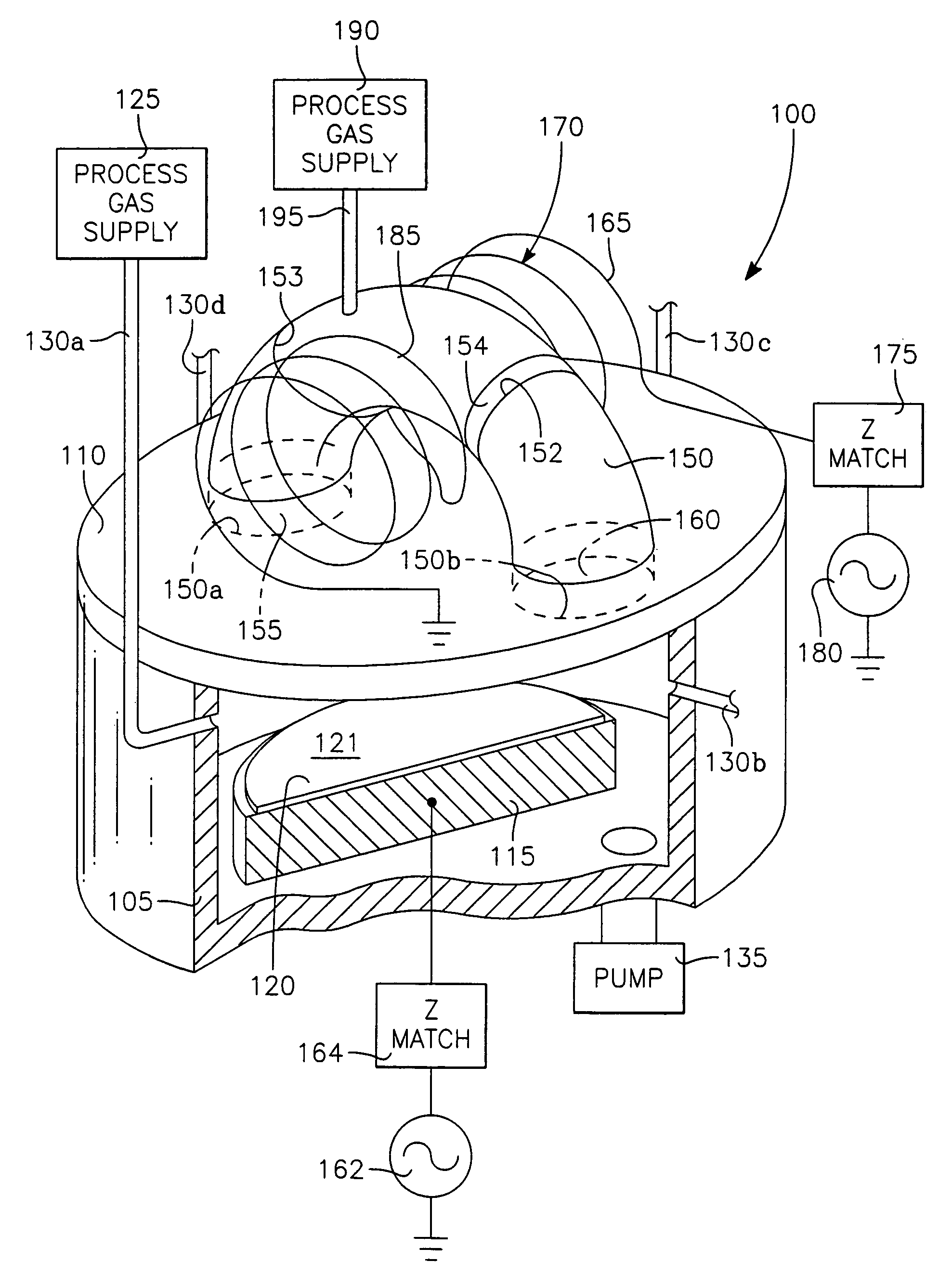
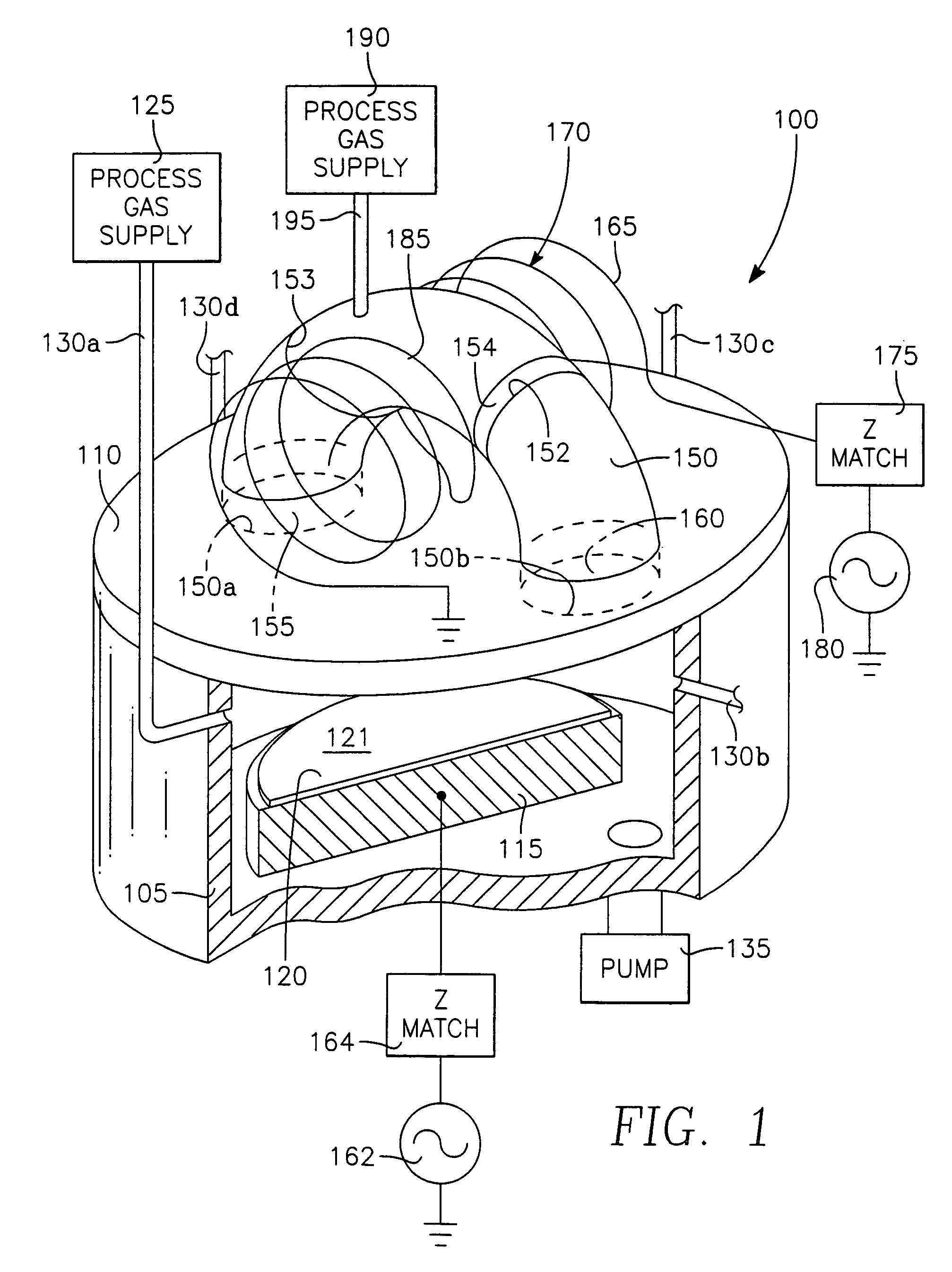
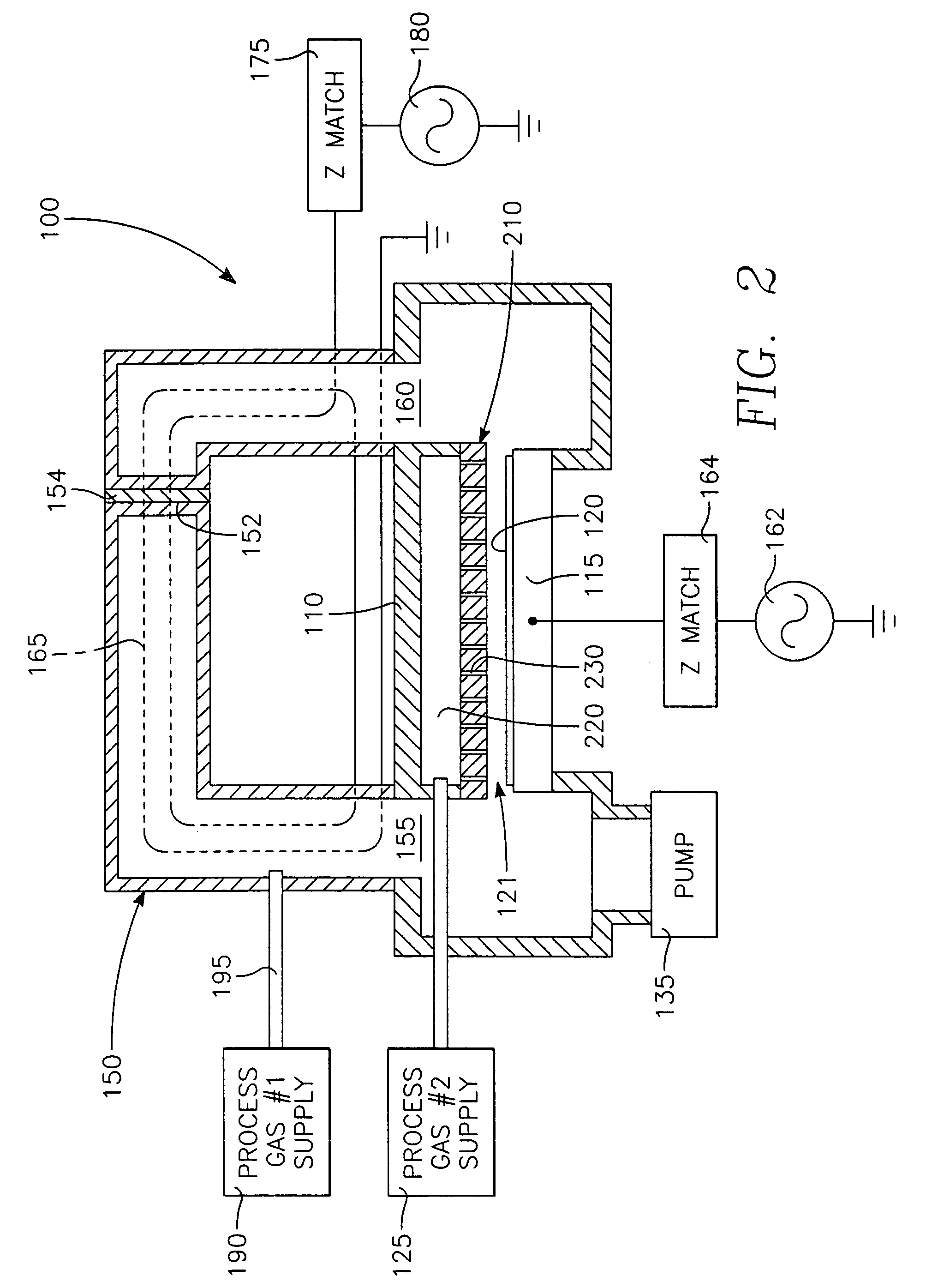
A method for implanting ions in a surface layer of a workpiece includes placing the workpiece on a workpiece support in a chamber with the surface layer being in facing relationship with a ceiling of the chamber, thereby defining a processing zone between the workpiece and the ceiling, and introducing into the chamber a process gas which includes the species to be implanted in the surface layer of the workpiece. The method further includes generating from the process gas a plasma by inductively coupling RF source power into the processing zone from an RF source power generator through an inductively coupled RF power applicator, and applying an RF bias from an RF bias generator to the workpiece support.

Description

CROSS-REFERENCE TO RELATED APPLICATIONS[0001]This application is a continuation-in-part of U.S. application Ser. No. 10 / 164,327 filed Jun. 5, 2002 by Kenneth Collins et al., entitled EXTERNALLY EXCITED TORROIDAL PLASMA SOURCE WITH MAGNETIC CONTROL OF ION DISTRIBUTION, which is a continuation-in-part of U.S. application Ser. No. 09 / 636,435, filed Aug. 11, 2000, entitled EXTERNALLY EXCITED MULTIPLE TORROIDAL PLASMA SOURCE by Hiroji Hanawa, et al., issued as U.S. Pat. No. 6,494,986 B1 on Dec. 17, 2002 and assigned to the present assignee.[0002]The following applications contain subject matter related to the present application:[0003]U.S. patent application Ser. No. 10 / 646,458, filed Aug. 22, 2003, entitled “PLASMA IMMERSION ION IMPLANTATION APPARATUS INCLUDING A PLASMA SOURCE HAVING LOW DISSOCIATION AND LOW MINIMUM PLASMA VOLTAGE” by Kenneth Collins, et al.; U.S. patent application Ser. No. 10 / 646,533, filed Aug. 22, 2003, entitled “PLASMA IMMERSION ION IMPLANTATION PROCESS USING A PLA...

Claims


Application Information

Patent Timeline
Patent Type & Authority Patents(United States)
IPC IPC(8): H01L21/42H01L21/425H01J37/32
CPCH01J37/321H01J37/32082
Inventor COLLINS, KENNETH S.HANAWA, HIROJIRAMASWAMY, KARTIKNGUYEN, ANDREWAL-BAYATI, AMIRGALLO, BIAGIOMONROY, GONZALO ANTONIO
Owner APPLIED MATERIALS INC
Learn More