Uses of self-organized needle-type nanostructures

a nanostructure and self-organized technology, applied in nanotechnology, magnetic recording, sensing record carriers, etc., to achieve the effect of improving power and good processability

Active Publication Date: 2010-05-13
X FAB SEMICON FOUNDRIES
View PDF9 Cites 33 Cited by
  • Summary
  • Abstract
  • Description
  • Claims
  • Application Information

AI Technical Summary

Benefits of technology

[0007]The present inventions are based on the object of indicating processes and components, the nanostructures being integrable in a reliab

Problems solved by technology

Due to the great differences of the impedances and/or the refractive indices of air and the semi-conductor material such as

Method used


Image

  • Uses of self-organized needle-type nanostructures
  • Uses of self-organized needle-type nanostructures
  • Uses of self-organized needle-type nanostructures

Examples


Embodiment Construction

[0138]With reference to FIGS. 1a to 1j and 9a, 9b example-like nanostructures and illustrative processes for their production are first of all elucidated. Then, similar processes and nanostructures can also be used in other applications, e.g. photoelectric components, sensor components, as optical coating structures in optical devices, as optical windows and the like, as this was already set forth above and will also be described in the following embodiments. Moreover, the nanostructures as they are e.g. produced by means of the processes described in the following may also be subjected to further treatments for the application of protective layers, the modification of the surface and the like.

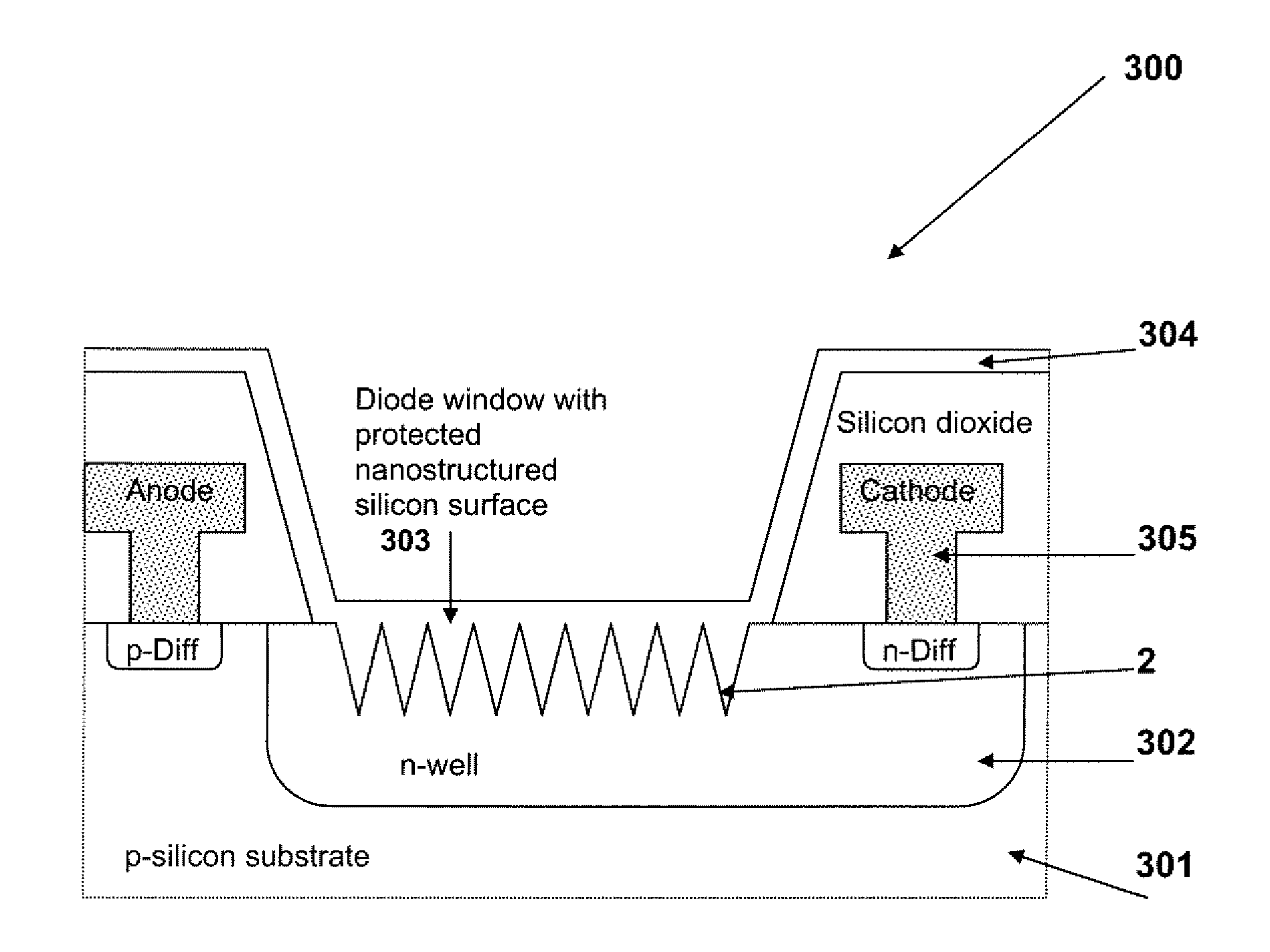
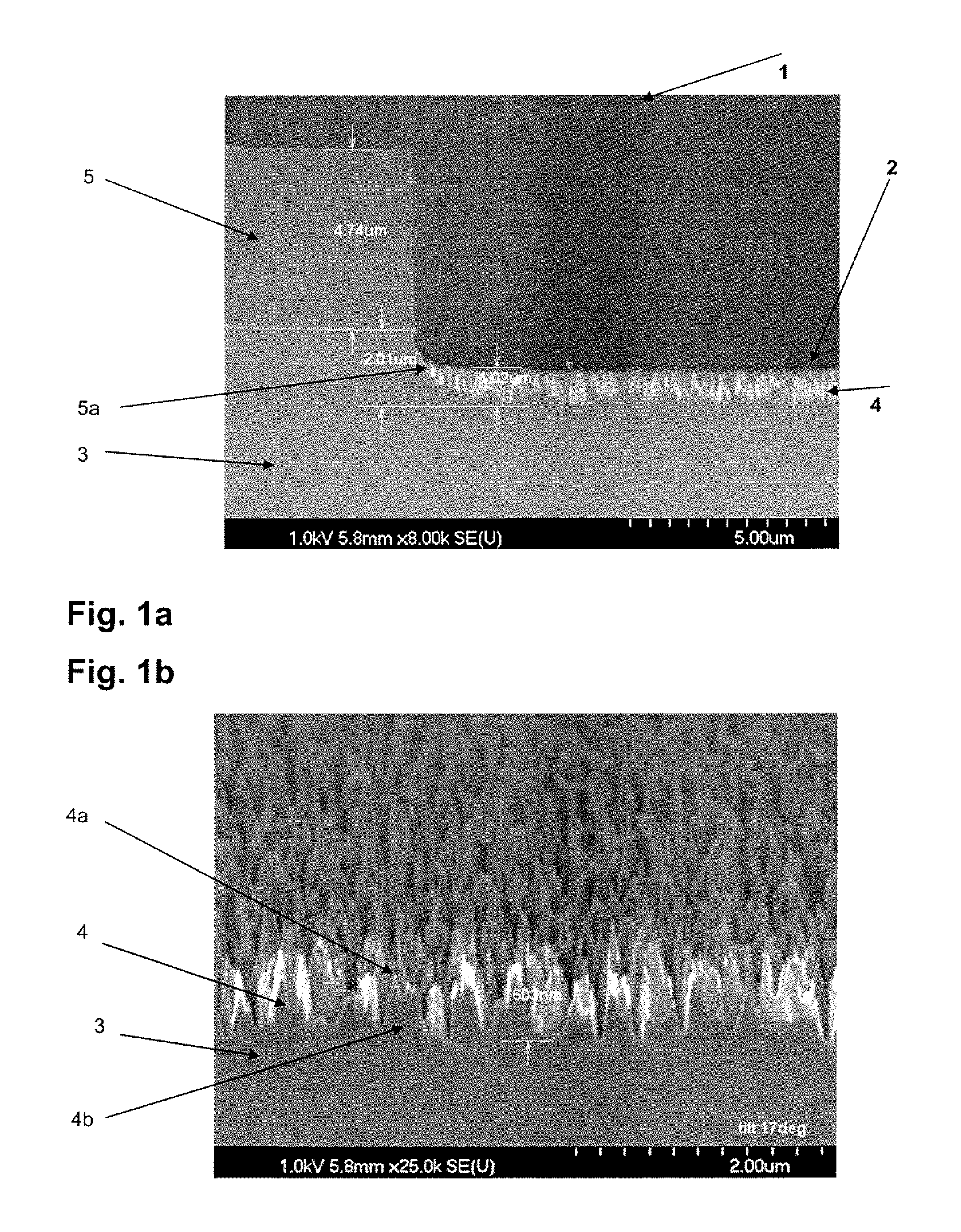
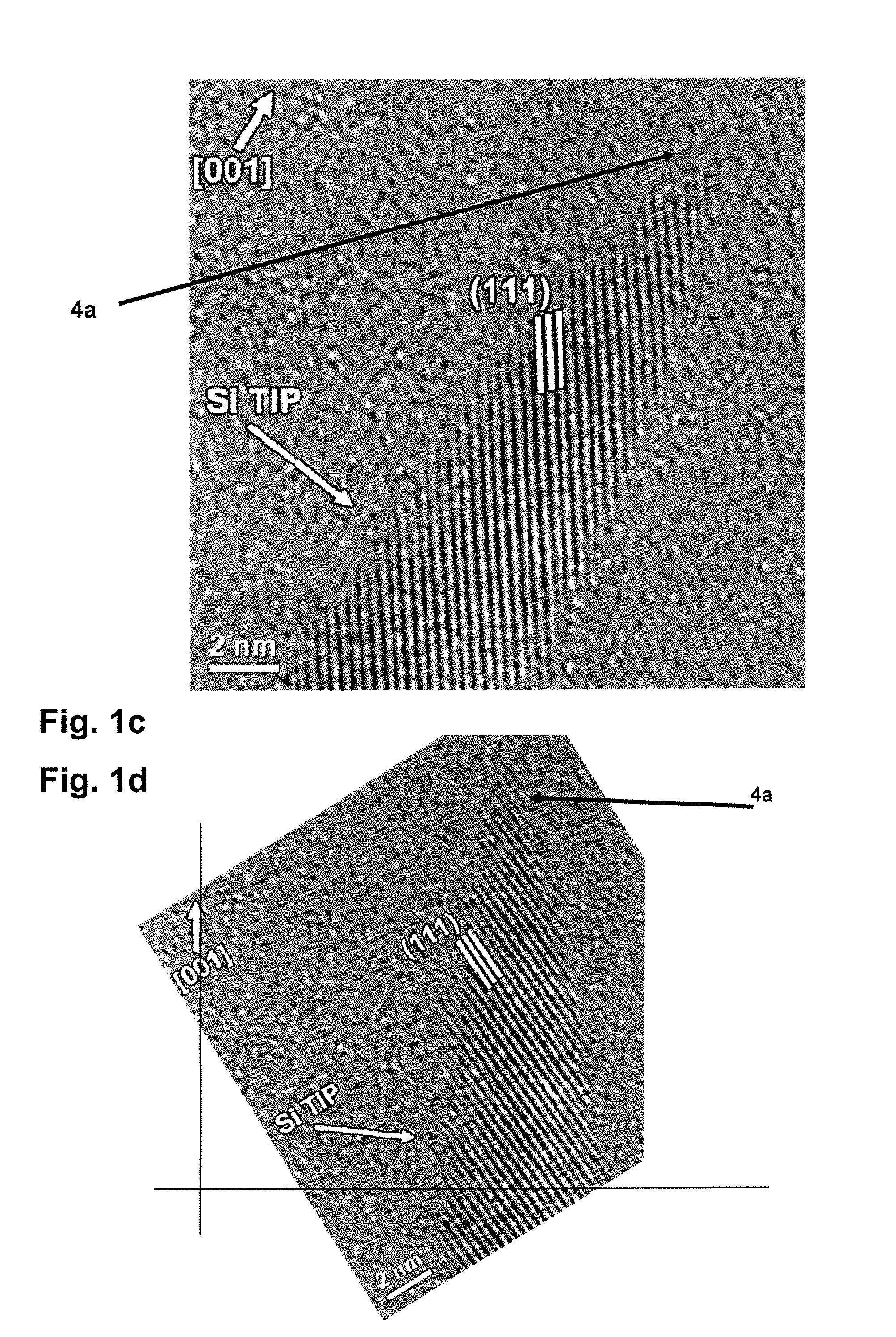
[0139]FIG. 1a shows a silicon-containing component 1 with a nanostructure 2 which has a monocrystalline silicon base layer 3 on which needle-type silicon structures 4 which are also alternatively (however as a synonym) designated as structural elements of the nanostructure 2 in this applicatio...


PUM


Abstract

The invention relates to processes for the production and elements (components) with a nanostructure (2; 4, 4a) for improving the optical behavior of components and devices and/or for improving the behavior of sensors by enlarging the active surface area. The nanostructure (2) is produced in a self-masking fashion by means of RIE etching and its material composition can be modified and it can be provided with suitable cover layers.

Description

FIELD OF THE INVENTION(S)[0001]The invention relates in general to the production of structured surfaces and in particular to the production of needle-type structures with nanodimensions, e.g., in the range below the wavelength of visible light, these structures being designated in the following as nanostructures. Their possibilities and technical applications are given special emphasis here.BACKGROUND INFORMATION[0002]Many electronic, optoelectronic, sensoric and micromechanical components have as a component silicon in doped and / or non-doped, crystalline and / or polycrystalline and / or amorphous form. In order to fulfill the component-specific requirements, silicon, may consequently be accordingly processed, which frequently includes a structuring of the silicon.[0003]In general, a mask made of photoresist is made for the structuring of silicon, by means of which the removal by means of an etching process is controlled. In order to produce small structures by means of a photoresist ...

Claims


Application Information

Patent Timeline
IPC IPC(8): H01L33/00B32B3/10B29D11/00B05D5/06G02B5/22H01L31/0232H01L21/3065
CPCB82Y20/00G02B1/118G02B2207/101H01L31/0216Y10T428/24355H01L31/0232H01L31/0236Y02E10/50H01L31/02165H01L31/02161H01L31/103H01L31/02363
Inventor GAEBLER, DANIELBACH, KONRAD
Owner X FAB SEMICON FOUNDRIES
Why Eureka
Try Eureka