Electroluminescent display initial-nonuniformity-compensated drive signal

a technology of non-uniformity and drive signal, applied in the field of initial non-uniformity-compensated drive signal of electroluminescent display, can solve the problems of oled display suffering from visible non-uniformity across the display, limiting the quality of the display, objectionable non-uniformity, etc., to achieve the effect of increasing the yield of good panels, not reducing the aperture ratio of subpixels, and simplifying the compensation of control signals

Active Publication Date: 2010-05-20
GLOBAL OLED TECH
View PDF17 Cites 27 Cited by
  • Summary
  • Abstract
  • Description
  • Claims
  • Application Information

AI Technical Summary

Benefits of technology

[0021]The present invention provides an effective way of providing the analog drive transistor control signal. It requires only one measurement to perform compensation. It can be applied to any active-matrix backplane. The compensation of the control signal has been simplified by using a look-up table (LUT) to change signals from nonlinear to linear so compensation can be in linear voltage domain. It compensates for initial nonuniformity without requiring complex pixel circuitry or external measurement devices. It does not decrease the aperture ratio of a subpixel. It has no effect on the normal operation of the panel. It can raise yield of good panels by making objectionable initial nonuniformity invisible.

Problems solved by technology

However, such displays suffer from a variety of defects that limit the quality of the displays.
In particular, OLED displays suffer from visible nonuniformities across a display.
This produces objectionable nonuniformity.
Further, nonuniform OLED material deposition can produce emitters with varying efficiencies, also causing objectionable nonuniformity.
This results in unacceptable display performance.
The measurement techniques are iterative, and therefore slow.
However, this approach will lead to an overall reduction in the dynamic range and brightness of the display and a reduction and variation in the bit depth at which the pixels can be operated.
However, the described approaches require either a lookup table providing a complete characterization for each pixel, or extensive computational circuitry within a device controller.
This is likely to be expensive and impractical in most applications.
Although this apparatus can correct for initial nonuniformity, it uses a sense resistor to measure current, and thus has limited signal-to-noise performance.
Furthermore, the measurements required by this method can be very time-consuming for large panels.
Such a process is time-consuming and requires mechanical fixtures to acquire the plurality of sub-area images.
However, their method requires a large number of LUTs, not all of which are in use at any given time, to perform processing and does not describe a method for populating those LUTs.
However, this method assumes a linear input and is consequently difficult to integrate with image-processing paths having nonlinear outputs.
However, this technique is only applicable to passive-matrix displays, not to the higher-performance active-matrix displays which are commonly employed.

Method used


Image

  • Electroluminescent display initial-nonuniformity-compensated drive signal
  • Electroluminescent display initial-nonuniformity-compensated drive signal
  • Electroluminescent display initial-nonuniformity-compensated drive signal

Examples


Embodiment Construction

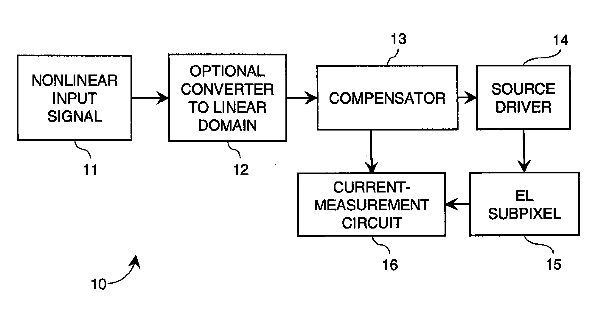
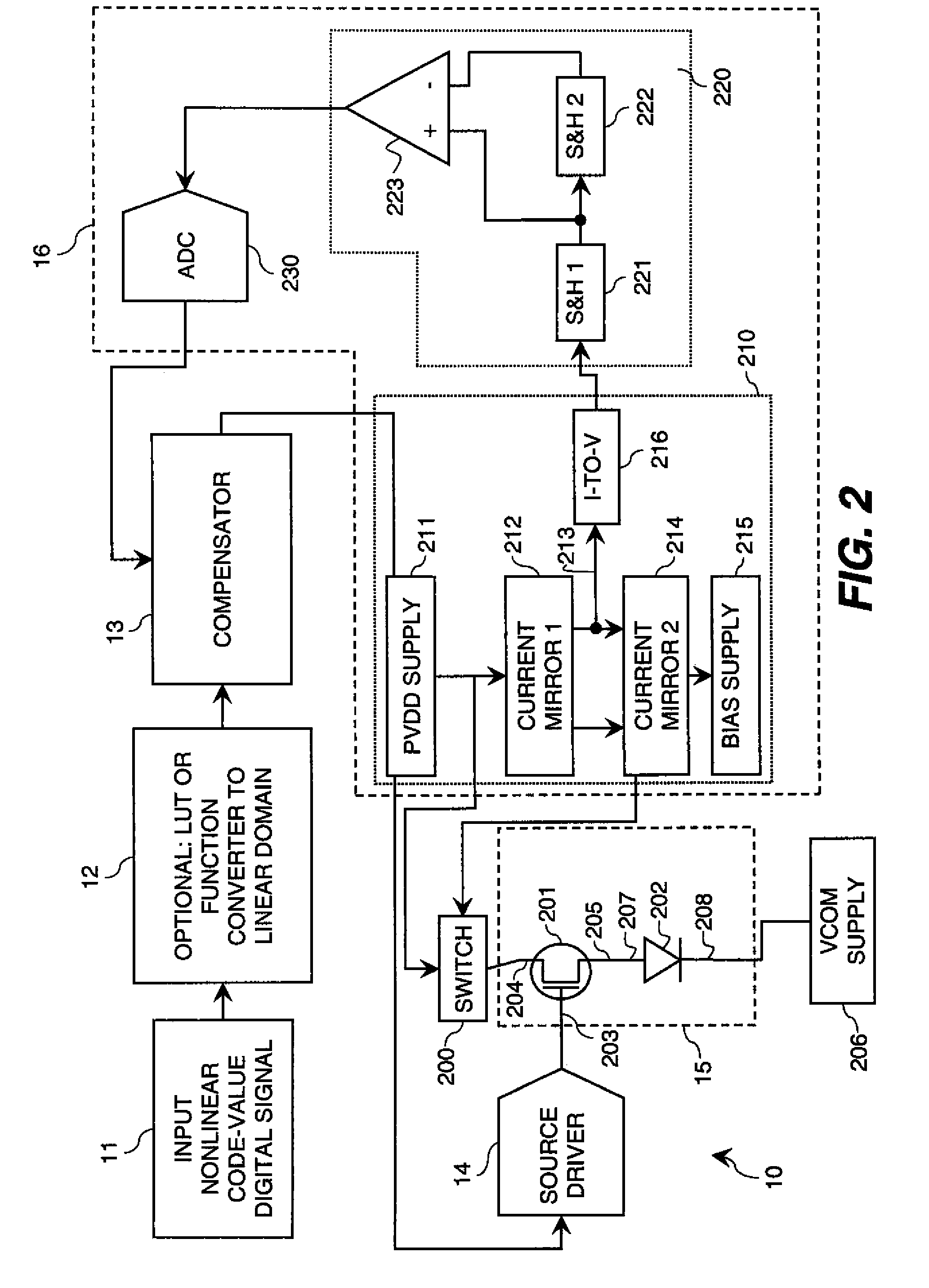
[0033]The present invention compensates for initial nonuniformity of all subpixels on an electroluminescent (EL) panel, e.g. an active-matrix OLED panel. A panel includes a plurality of pixels, each of which includes one or more subpixels. For example, each pixel might include a red, a green, and a blue subpixel. Each subpixel includes an EL emitter, which emits light, and surrounding electronics. A subpixel is the smallest addressable element of a panel.

[0034]The discussion to follow first considers the system as a whole. It then proceeds to the electrical details of a subpixel, followed by the electrical details for measuring one subpixel and the timing for measuring multiple subpixels. It next covers how the compensator uses measurements. Finally, it describes how this system is implemented in one embodiment, e.g. in a consumer product, from the factory to end-of-life.

Overview

[0035]FIG. 1 shows a block diagram of the display system 10 of the present invention. This figure shows d...


PUM


Abstract

An electroluminescent (EL) panel with 2T1C subpixels is compensated for initial nonuniformity (“mura”). The current of each subpixel is measured at a selected time to provide a status signal representing the characteristics of the subpixel. A compensator receives a linear code value and changes it according to the status signals. A linear source driver drives the panel with the changed code values.

Description

CROSS REFERENCE TO RELATED APPLICATIONS[0001]Reference is made to commonly-assigned, co-pending U.S. patent application U.S. Ser. No. 11 / 962,182 entitled “ELECTROLUMINESCENT DISPLAY COMPENSATED ANALOG TRANSISTOR DRIVE SIGNAL” to Leon et al, filed Dec. 21, 2007, incorporated by reference herein.FIELD OF THE INVENTION[0002]The present invention relates to control of an analog signal applied to a drive transistor for supplying current through an electroluminescent emitter.BACKGROUND OF THE INVENTION[0003]Flat-panel displays are of great interest as information displays for computing, entertainment, and communications. For example, electroluminescent (EL) emitters have been known for some years and have recently been used in commercial display devices. Such displays employ both active-matrix and passive-matrix control schemes and can employ a plurality of subpixels. Each subpixel contains an EL emitter and a drive transistor for driving current through the EL emitter. The subpixels are ...

Claims


Application Information

Patent Timeline
Patent Type & Authority Applications(United States)
IPC IPC(8): G06F3/038
CPCG09G3/2092G09G3/3233G09G2300/0842G09G2320/0233G09G2320/0285G09G2360/16G09G2320/0295G09G2320/043G09G2320/045G09G2320/0693G09G2320/029G09G3/20G09G3/32
Inventor LEON, FELIPE A.WHITE, CHRISTOPHER J.PARRETT, GARYPRIMERANO, BRUNO
Owner GLOBAL OLED TECH
Why Eureka
Try Eureka