Self-Aligned Three-Dimensional Non-Volatile Memory Fabrication

Active Publication Date: 2010-05-20
SANDISK TECH LLC
View PDF35 Cites 30 Cited by
  • Summary
  • Abstract
  • Description
  • Claims
  • Application Information

AI Technical Summary

Benefits of technology

[0015]A silicide process for forming conductors is also provided. Silicon can be etched to form conductor array lines for a memory array, followed by a silicidization process to form low resistance structures. Additional t

Problems solved by technology

Numerous processing difficulties may exist in the formation of these structures.
However, etching through a significant number of layers in a single etch process can pose its own set

Method used


Image

  • Self-Aligned Three-Dimensional Non-Volatile Memory Fabrication
  • Self-Aligned Three-Dimensional Non-Volatile Memory Fabrication
  • Self-Aligned Three-Dimensional Non-Volatile Memory Fabrication

Examples


Embodiment Construction

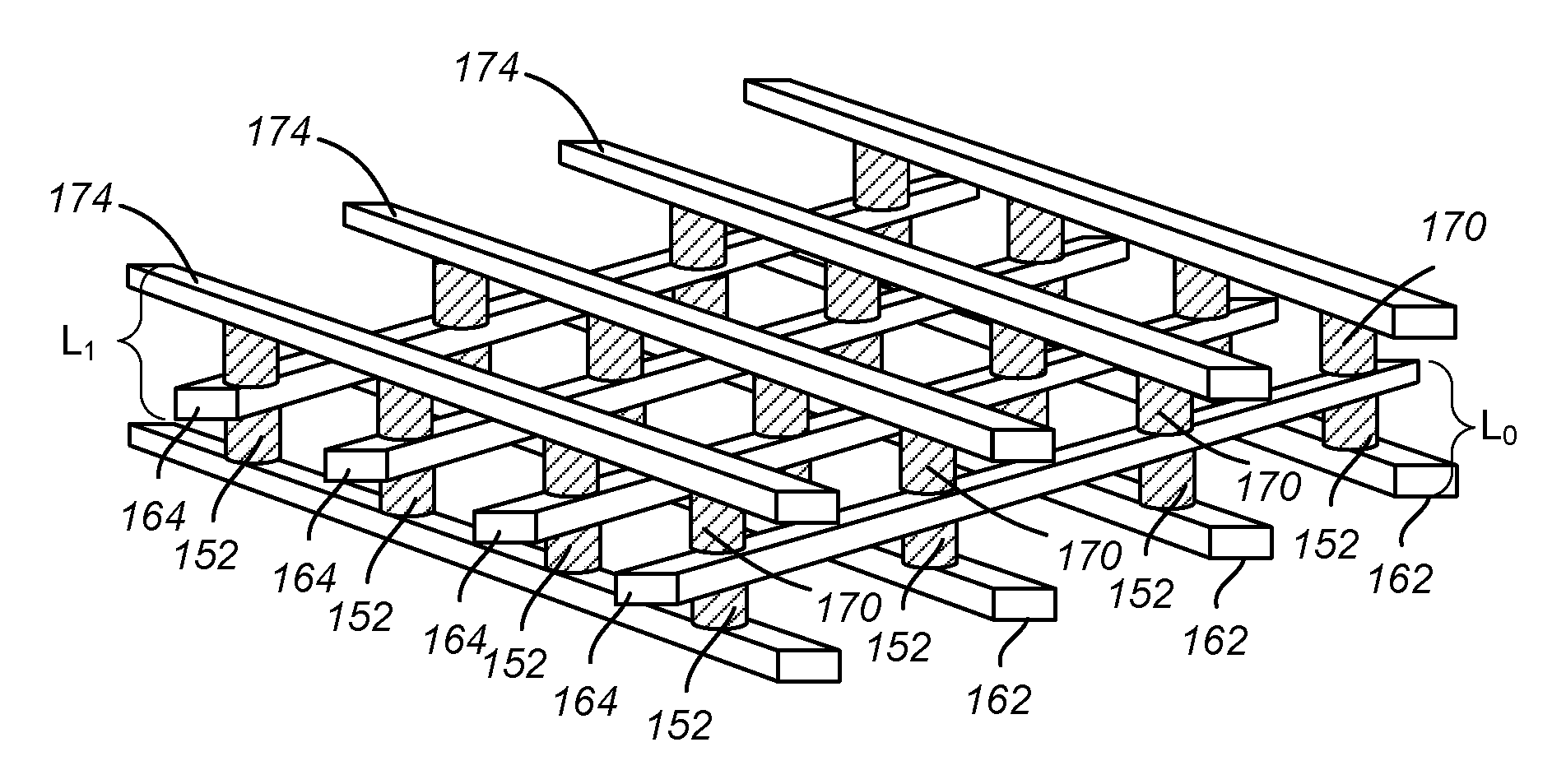
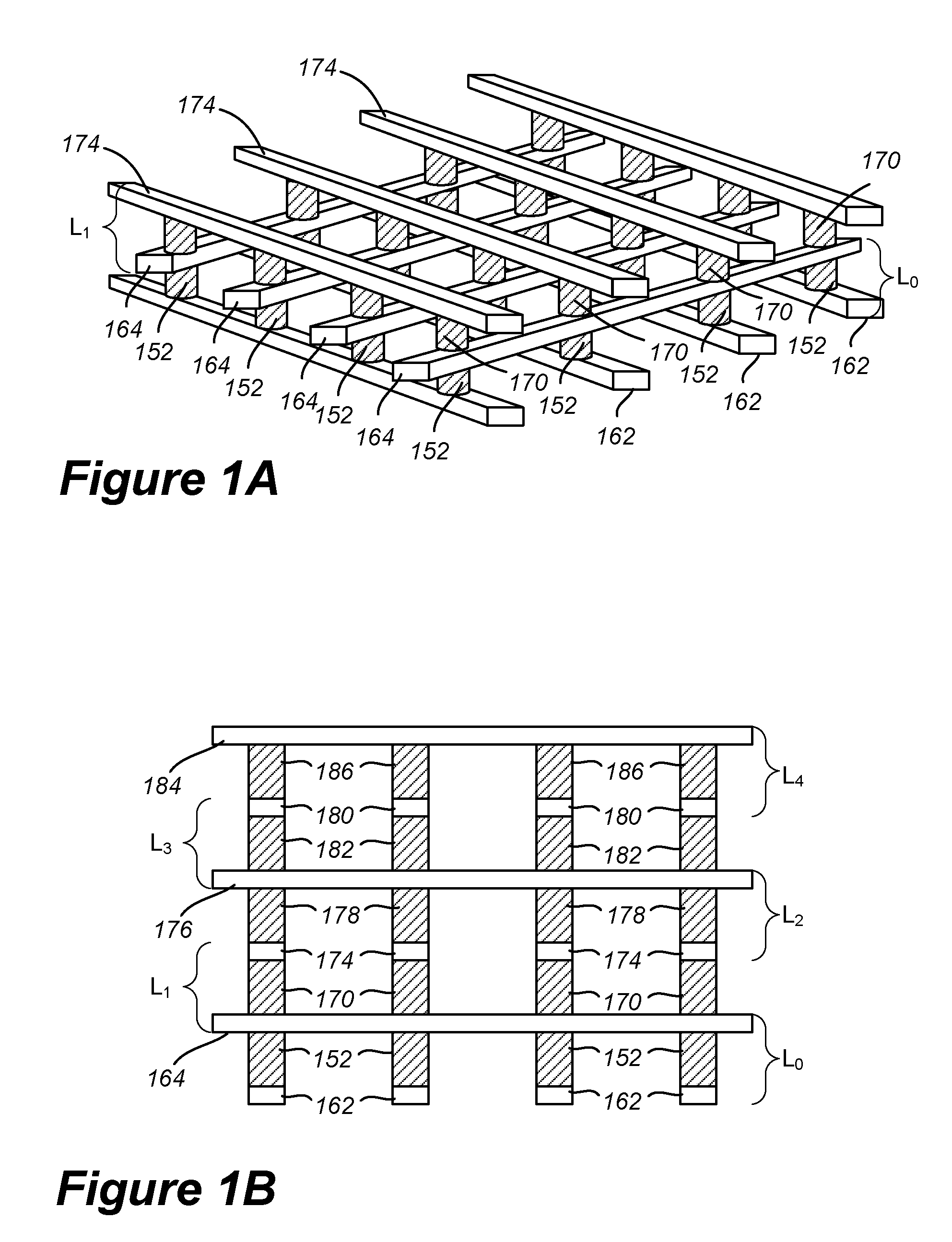
[0032]FIGS. 3A-3H are schematic illustrations of a fabrication sequence for a monolithic non-three-dimensional non-volatile memory array in accordance with one embodiment of the presently disclosed technology. Conceptually, the disclosed technique includes a double etch process in the same direction for each of the conductor layers except the first conductor layer. A semiconductor layer stack and underlying conductor layer are patterned in a first direction (e.g., north-to-south) and etched into strips elongated in a second orthogonal direction (e.g., east-to-west). A second conductor layer is then deposited and patterned in the second direction before forming a second semiconductor layer stack. The second conductor layer is etched into strips elongated in the first direction and the layer stack strips are etched into pillars. A third conductor layer is then deposited, followed by a second semiconductor layer stack. A third pattern is then formed, also in the second direction. The s...


PUM

PropertyMeasurementUnit
Electrical conductivityaaaaaaaaaa
Electrical resistanceaaaaaaaaaa
Electrical conductoraaaaaaaaaa

Abstract

A self-aligned fabrication process for three-dimensional non-volatile memory is disclosed. A double etch process forms conductors at a given level in self-alignment with memory pillars both underlying and overlying the conductors. Forming the conductors in this manner can include etching a first conductor layer using a first repeating pattern in a given direction to form a first portion of the conductors. Etching with the first pattern also defines two opposing sidewalls of an underlying pillar structure, thereby self-aligning the conductors with the pillars. After etching, a second conductor layer is deposited followed by a semiconductor layer stack. Etching with a second pattern that repeats in the same direction as the first pattern is performed, thereby forming a second portion of the conductors that is self-aligned with overlying layer stack lines. These layer stack lines are then etched orthogonally to define a second set of pillars overlying the conductors.

Description

CLAIM OF PRIORITY[0001]The present application claims priority from U.S. Provisional Patent Application No. 61 / 115,913, entitled “SELF-ALIGNED STACKED MEMORY ARRAYS AND METHODS OF FORMING,” by Matamis et al., filed Nov. 18, 2008, incorporated by reference herein in its entirety.BACKGROUND OF THE INVENTION[0002]1. Field of the Invention[0003]Embodiments in accordance with the present disclosure are directed to integrated circuits containing non-volatile memory cell arrays and particularly those arrays incorporating passive element memory cells.[0004]2. Description of the Related Art[0005]Materials having a detectable level of change in state, such as a resistance or phase change, are used to form various types of non-volatile semiconductor based memory devices. For example, simple antifuses are used for binary data storage in one time field-programmable (OTP) memory arrays by assigning a lower resistance initial physical state of a memory cell to a first logical state such as logical...

Claims


Application Information

Patent Timeline
IPC IPC(8): H01L21/20H01L21/3205
CPCG11C13/0004H01L45/1675G11C2213/71G11C2213/72H01L27/101H01L27/1021H01L27/2409H01L27/2463H01L27/2481H01L45/04H01L45/06H01L45/085H01L45/1233H01L45/144H01L45/146H01L45/147G11C17/16H10B63/84H10B63/20H10B63/80H10N70/245H10N70/20H10N70/8836H10N70/231H10N70/8828H10N70/8833H10N70/063H10N70/826H01L21/20
Inventor MATAMIS, GEORGECHIEN, HENRYKAI, JAMES K.ORIMOTO, TAKASHIPURAYATH, VINOD RPING, ER-XUANSCHEUERLEIN, ROY E.
Owner SANDISK TECH LLC
Why Eureka
Try Eureka