Process for fabricating piezoelectric element

Active Publication Date: 2010-05-27
PANASONIC CORP
View PDF7 Cites 7 Cited by
  • Summary
  • Abstract
  • Description
  • Claims
  • Application Information

AI Technical Summary

Benefits of technology

[0008]The invention is aimed to provide a production method of a piezoelectric element in which generation of an electric field in a piezoelectric thin film layer is avoided during a manufacturing process, securing a high piezoelectric properties or performance of the element.
[0009]The production method of the piezoelectric element of the invention includes first to fourth production processes. The first process is a depositing process for depositing an under electrode layer, piezoelectric thin film layer and an upper electrode layer successively on a substrate. The second process is etching process including dry etching. The third process is polarization p

Problems solved by technology

When a voltage is applied across the under electrode layer and the upper electrode layer, the piezoelectric thin film layer expands and contracts, causing a mechanical displacement.
If an electric fi

Method used


Image

  • Process for fabricating piezoelectric element
  • Process for fabricating piezoelectric element
  • Process for fabricating piezoelectric element

Examples


Example

First Exemplary Embodiment

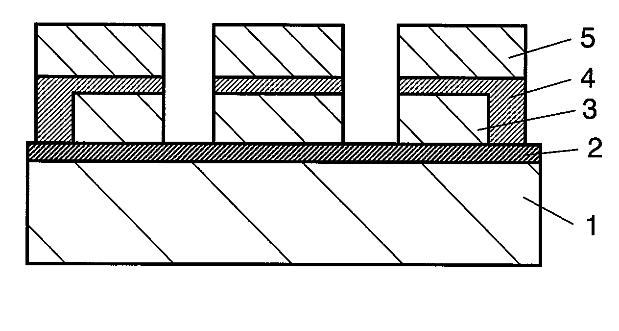
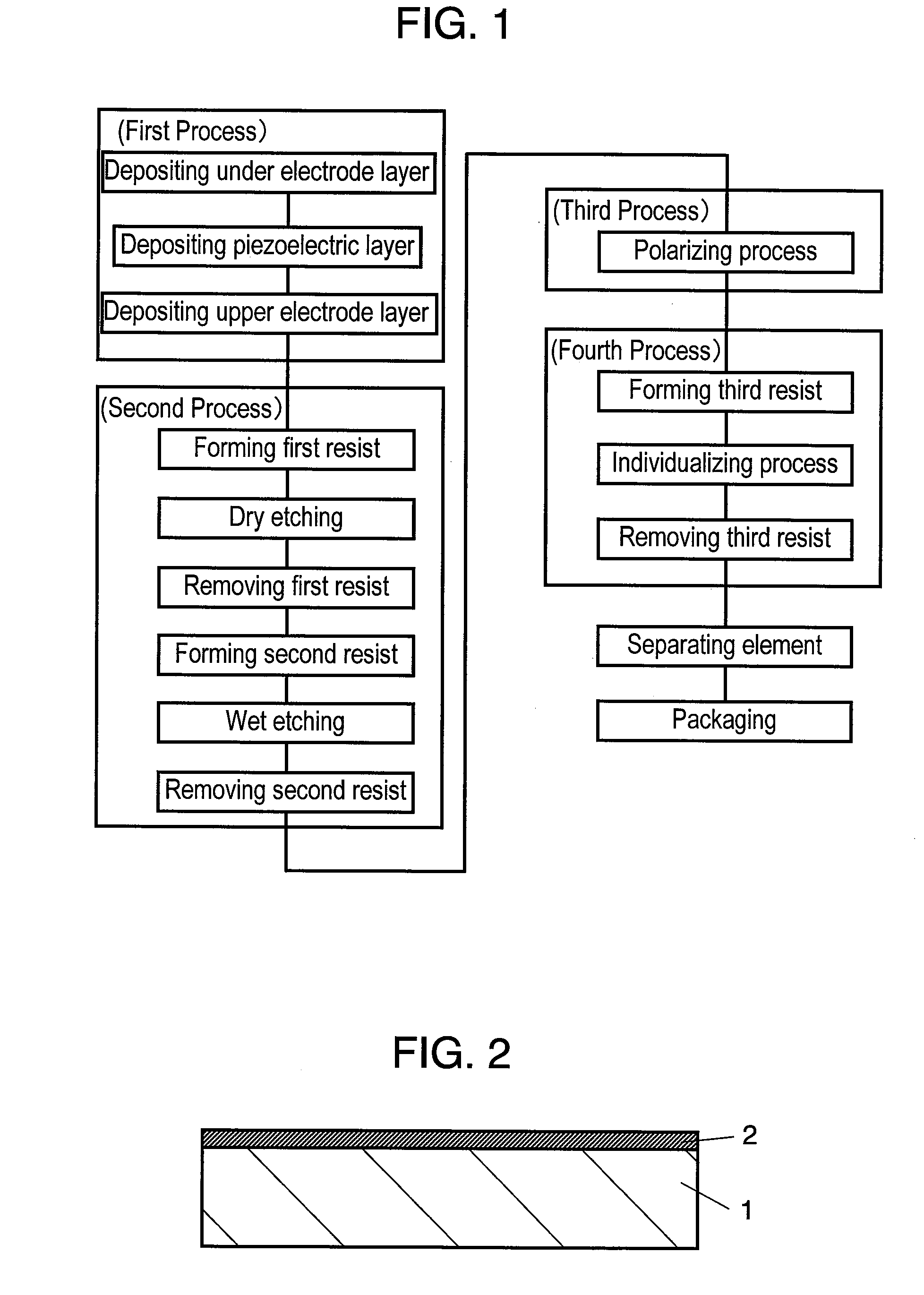
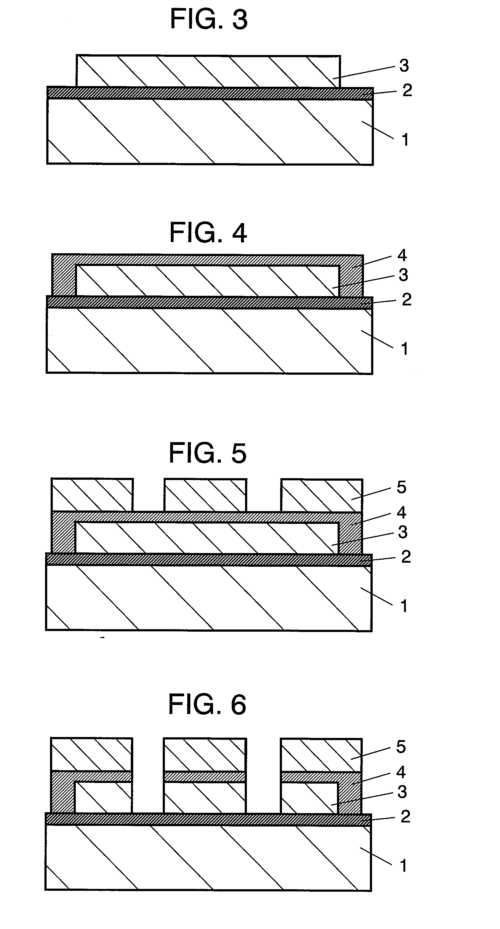
[0045]FIG. 1 is a flow chart showing a production method of a piezoelectric element in accordance with the first exemplary embodiment of the invention. FIGS. 2 to 15 are cross sectional views of the piezoelectric element explaining a first to a fourth process of the production method. Each manufacturing process is explained below along with the flow chart in FIG. 1. In considering a lot production of piezoelectric elements, under electrodes and upper electrodes of each element are preferably connected equipotentially. For explaining the exemplary embodiment, the drawings show cross-sectional structures of three pieces of piezoelectric element for each production process.

[0046]In the first process shown in FIG. 2, forming under electrode layer 2 on Si substrate 1 made of silicon so as Pt is deposited to be crystallized in direction. As an ordinary method of forming under electrode layer 2, platinum (Pt) is sputtered, Pt and titanium (Ti) are sputtered at th...

Example

Second Exemplary Embodiment

[0066]FIG. 16 is a flow chart showing a production method of a piezoelectric element in accordance with the second exemplary embodiment of the invention. FIGS. 17 to 21 are cross sectional views illustrating the production method of the piezoelectric element in the second exemplary embodiment and which are explained with reference to the flow chart in FIG. 16. The production method according to the second embodiment is greatly different from the first exemplary embodiment, and under electrode layer 2 and upper electrode layer 4 once opened just before the polarization process are short-circuited again after polarization process. With this arrangement, polarization state or direction is stably maintained and occurrence of static destruction or pyroelectric destruction is avoided. As a result, in the production method, polarization state or direction after the polarization is more securely maintained even up to the final stage of completing the piezoelectric...


PUM

PropertyMeasurementUnit
Electrical conductoraaaaaaaaaa
Electric potential / voltageaaaaaaaaaa

Abstract

A method for fabricating a piezoelectric element capable of ensuring high piezoelectric characteristics by preventing generation of unnecessary electric field in a piezoelectric thin film layer during the fabrication process. The method for fabricating a piezoelectric element comprises a first step for depositing a lower electrode layer, a piezoelectric thin film layer and an upper electrode layer sequentially on a substrate, a second step for performing etching including dry etching, a third step for performing polarization by applying a voltage between the lower electrode layer and the upper electrode layer, and a fourth step for segmenting into individual piezoelectric elements wherein the lower electrode layer and the upper electrode layer are held in short circuit state at least when dry etching is performed.

Description

TECHNICAL FIELD[0001]This invention relates to a production method of a piezoelectric element using a piezoelectric thin film to be used for a sensor, an actuator or the like.BACKGROUND OF ART[0002]A piezoelectric thin film made of ferroelectrics in a perovskite-type structure has a superb dielectric, piezoelectric and pyroelectric effect, and is expected to be widely used for a variety of piezoelectric devices including sensors, actuators and transducers. The piezoelectric thin film of ferroelectrics has inherently a spontaneous polarization. When stress is applied to the piezoelectric thin film, the polarization state is changed by strain and which is detected as a current. When a voltage is applied to the thin film, the film expands and contracts in response to an intensity of the applied voltage.[0003]A piezoelectric element using the piezoelectric thin film is produced by depositing an under electrode layer, a piezoelectric thin film layer and an upper electrode layer successiv...

Claims


Application Information

Patent Timeline
IPC IPC(8): H01L41/22B41J2/14H01L41/09B41J2/16H01L41/18H01L41/187H01L41/257H01L41/332
CPCH01L41/257H01L41/314Y10T29/49401Y10T29/42H01L41/332H10N30/045H10N30/082H10N30/80H10N30/00
Inventor NAKAMURA, YUKIMURASHIMA, YUJIYASUMI, MASAHIROKOMAKI, KAZUKI
Owner PANASONIC CORP
Why Eureka
Try Eureka