Method and structure for establishing contacts in thin film transistor devices

a thin film transistor and contact technology, applied in the direction of transistors, solid-state devices, semiconductor devices, etc., can solve the problems of contact problems, inability to achieve functional groups, and inability to work well with silane surface modification for many gate dielectrics

Active Publication Date: 2010-05-27
XEROX CORP
View PDF14 Cites 48 Cited by
  • Summary
  • Abstract
  • Description
  • Claims
  • Application Information

AI Technical Summary

Benefits of technology

[0010]In another aspect of the presently described emb...

Problems solved by technology

However, this silane surface modification does not work well for many gate dielectrics that do not have abundant hydroxyl groups at its surface, such as many polymer dielectrics.
A hydrophobic (polymer) layer can be deposited instead, but simply adding a hydrophobic layer also partially covers the source and drain electrodes and causes contact problems since such layer typically may be thicker than a monolayer.
Other gate dielectrics may b...

Method used


Image

  • Method and structure for establishing contacts in thin film transistor devices
  • Method and structure for establishing contacts in thin film transistor devices
  • Method and structure for establishing contacts in thin film transistor devices

Examples


Embodiment Construction

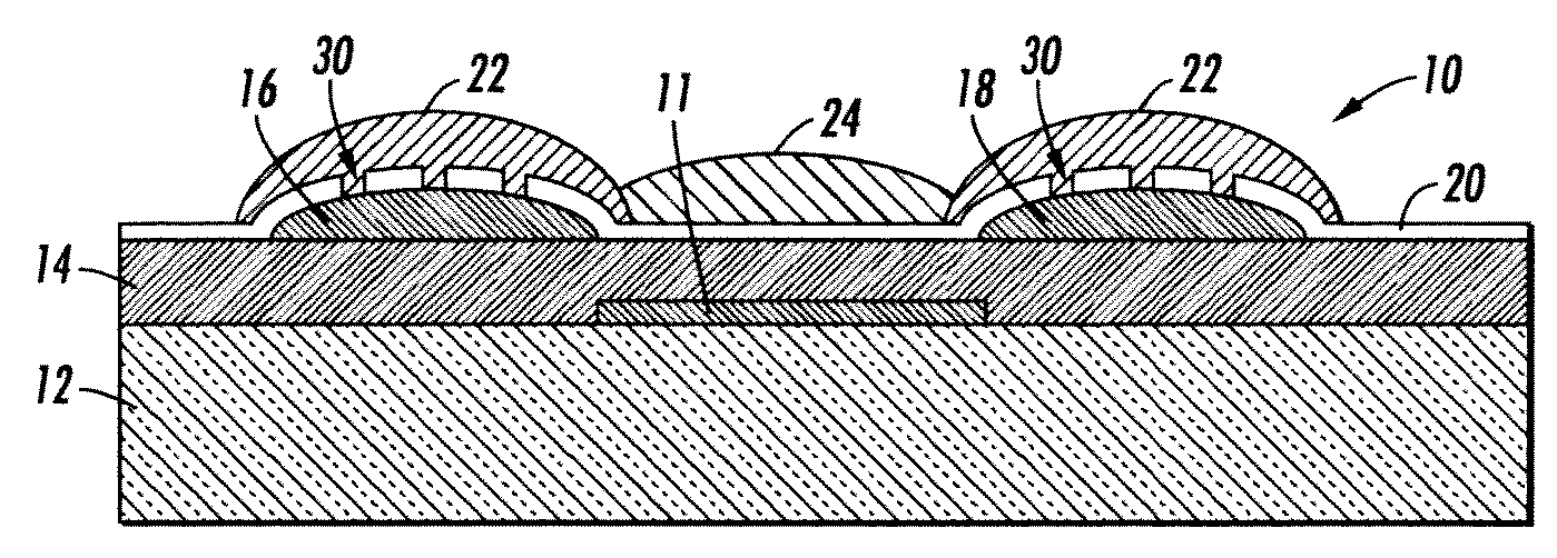
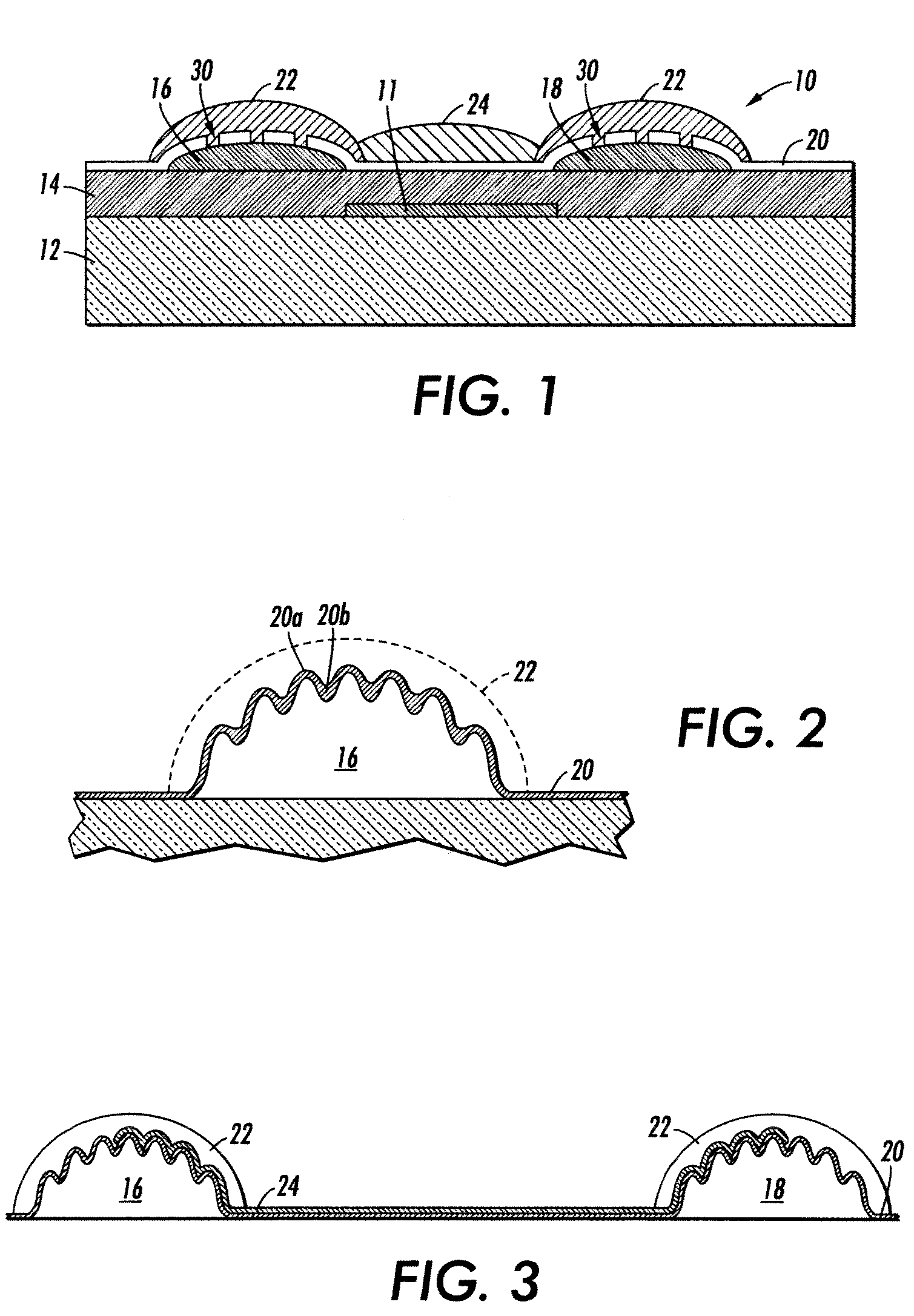
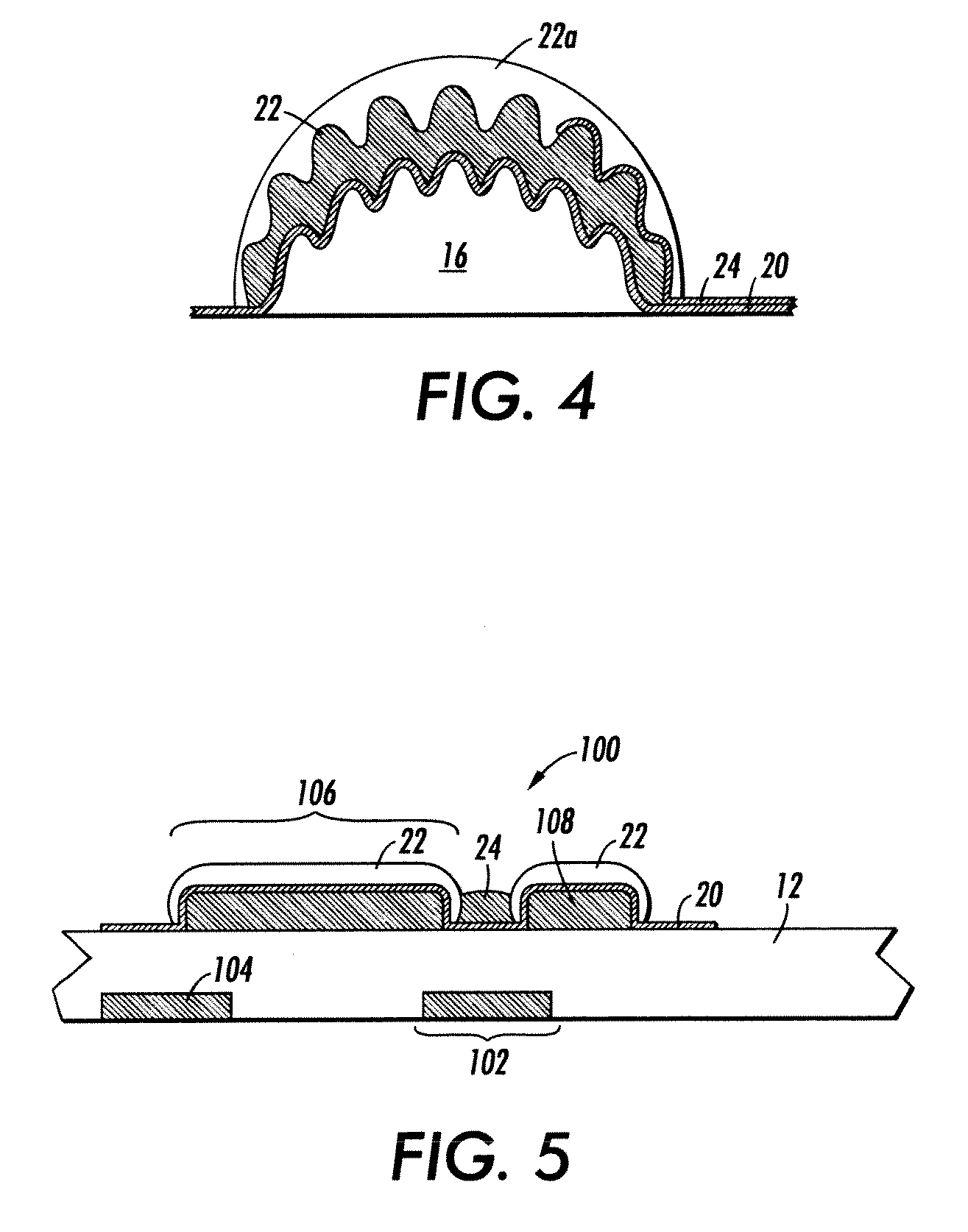
[0040]In the presently described embodiments, the roughness, surface discontinuity and / or structural height of printed metal lines is used to pin a fluid. In at least one form, this fluid deposits over a hydrophobic or low-surface-energy layer (including a hydrophobic polymer layer) and is connected to bottom contacts (including printed contacts) through pinholes in the low surface-energy layer or / and through charge tunneling through that layer. This results in a sandwich-like contact structure achieved in a self-aligned deposition process. In one form, improved source-drain contact results in thin film transistors (TFTs) formed using an all-additive process. Although the present technique is described for printed circuits based on thin film transistors, it may be applied to electrodes in general. For example, it may also be used in optical devices such as organic light emitting diodes, in sensors, such as light sensors, photovoltaic devices or in micro-fluidic devices for applicati...


PUM

PropertyMeasurementUnit
Electrical conductoraaaaaaaaaa
Areaaaaaaaaaaa
Semiconductor propertiesaaaaaaaaaa

Abstract

The roughness and structural height of printed metal lines is used to pin a fluid. This fluid deposits a top contact material which is connected to the bottom printed contacts through pinholes in the hydrophobic polymer layer. This results in a sandwich-like contact structure achieved in a self-aligned deposition process and having improved source-drain contact for all-additive printed circuits. In one form, the present technique is used for thin film transistor applications, but it may be applied to electrodes in general.

Description

CROSS REFERENCE TO RELATED PATENTS AND APPLICATIONS[0001]This application is related to U.S. application No. ______, filed on even date herewith, entitled, “Thin Film Transistors and High Fill Factor Pixel Circuits and Methods for Forming Same,” and naming Daniel et al. as inventors (bearing Attorney Docket No. 200610160-US-NP, XERZ 2 01743) and U.S. application No. ______, filed on even date herewith, entitled, “An Electronic Circuit Structure and Method for Forming Same,” and naming Daniel et al. as inventors (bearing Attorney Docket No. 20070476-US-NP, XERZ 2 01791).BACKGROUND[0002]The development of thin film transistors (TFTs) using printing techniques has uncovered a number of issues that should be addressed before large scale production of such devices becomes more prevalent. Typically, such devices have as one of its components a gate dielectric. So, for example, it has been found that a hydrophobic gate dielectric results in improved molecular ordering of the organic semico...

Claims


Application Information

Patent Timeline
IPC IPC(8): H01L29/786H01L21/336
CPCH01L29/1606H01L29/78684H01L29/7869H01L51/0003H01L51/0562H01L51/052H01L51/0541H01L51/0545H01L51/0558H01L51/0037H10K71/12H10K85/1135H10K10/471H10K10/466H10K10/486H10K10/464H10K10/484
Inventor DANIEL, JURGEN H.ARIAS, ANA CLAUDIACHABINYC, MICHAEL
Owner XEROX CORP
Why Eureka
Try Eureka