Non-volatile memory cell with self aligned floating and erase gates, and method of making same

a technology of floating gate and erase gate, which is applied in the direction of semiconductor devices, electrical devices, transistors, etc., can solve the problems of unfavorable high-voltage operation, difficult to surround the control gate with sufficient insulation, and unwanted capacitive coupling between the control gate and the floating ga

Active Publication Date: 2010-05-27
SILICON STORAGE TECHNOLOGY
View PDF49 Cites 23 Cited by
  • Summary
  • Abstract
  • Description
  • Claims
  • Application Information

AI Technical Summary

Benefits of technology

[0008]An electrically programmable and erasable memory device includes a substrate of semiconductor material having a first conductivity type and a surface, a trench formed into the surface of the substrate, first and second spaced-apart regions formed in the substrate and having a second conductivity type, with a channel region in the substrate there between, wherein the first region is formed under the trench, and the channel region includes a first portion that extends substantially along a sidewall of the trench and a second portion that extends substantially along the surface of the substrate, an electrically conductive floating gate at least partially disposed in the trench adjacent to and insulated from the channel region first portion for controlling a conductivity of the channel region first portion, an electrically conductive control gate disposed over and insulated from the channel region second portion for controlling a conductivity of the channel region second portion, and an electrically conductive erase gate disposed adjacent to and insulated from the floating gate.
[0009]An array of electrically programmable and erasable memory devices includes a substrate of semiconductor material having a first conductivity type and a surface, spaced apart isolation regions formed on the substrate which are substantially parallel to one another and extend in a first direction, with an active region between each pair of adjacent isolation regions, and each of the active regions including a plurality of pairs of memory cells. Each of the memory cell pairs includes a trench formed into the surface of the substrate and including a pair of opposing sidewalls, a first region formed in the substrate under the trench, a pair of second regions formed in the substrate, with a pair of channel regions each in the substrate between the first region and one of the second regions, wherein the first and second regions have a second conductivity type, and wherein each of the channel regions includes a first portion that extends substantially along one of the opposing trench sidewalls and a second portion that extends substantially along the substrate surface, a pair of electrically conductive floating gates each at least partially disposed in the trench adjacent to and insulated from one of the channel region first portions for controlling a conductivity of the one channel region first portion, an electrically conductive erase gate disposed adjacent to and insulated from the floating gates, and a pair of electrically conductive control gates each disposed over and insulated from one of the channel region second portions for controlling a conductivity of the one channel region second portion.
[0010]A method of forming a semiconductor me

Problems solved by technology

One of the problems facing the manufacturability of semiconductor floating gate memory cell arrays has been the alignment of the various components such as source, drain, control gate, and floating gate.
This means the control gate is both a low voltage and high voltage element, making it difficult to surround it w

Method used


Image

  • Non-volatile memory cell with self aligned floating and erase gates, and method of making same
  • Non-volatile memory cell with self aligned floating and erase gates, and method of making same
  • Non-volatile memory cell with self aligned floating and erase gates, and method of making same

Examples


Embodiment Construction

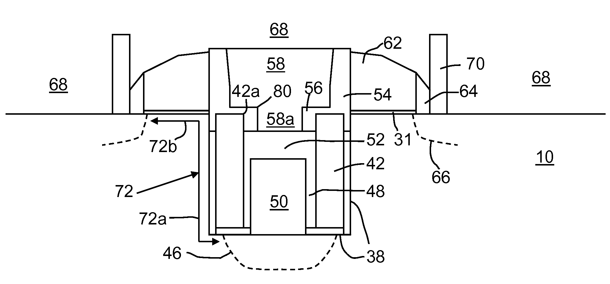
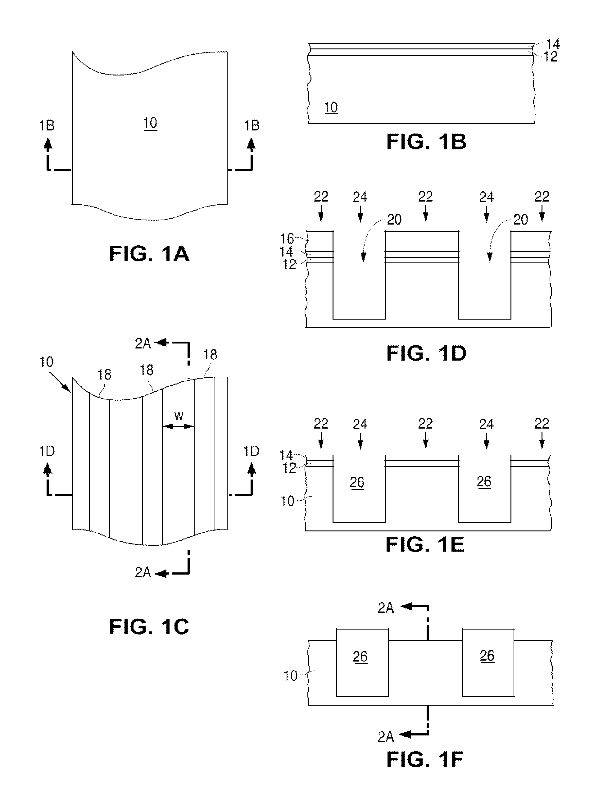
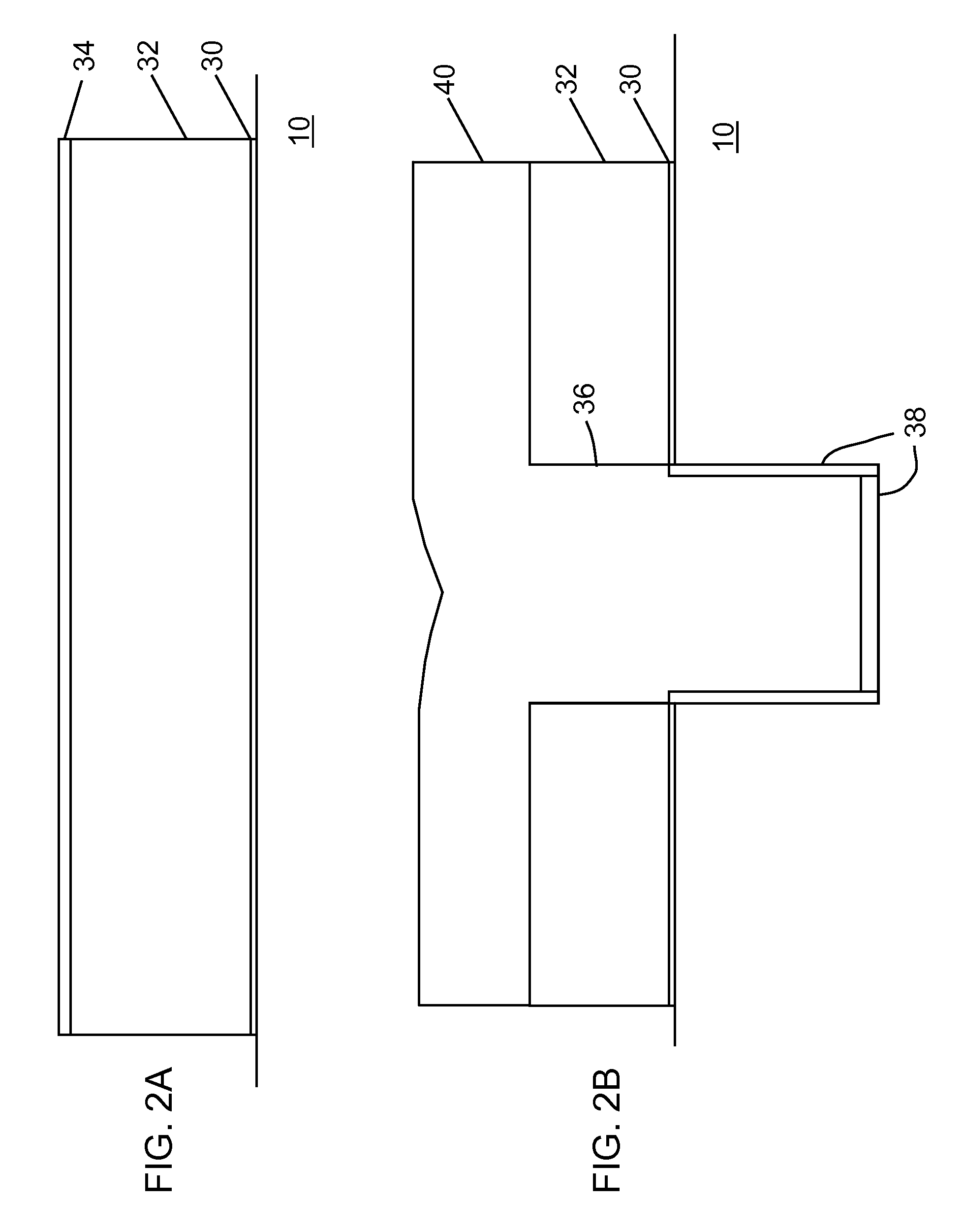
[0022]The method of the present invention is illustrated in FIGS. 1A to 1F and 2A to 2F (which show the processing steps in making the memory cell array of the present invention). The method begins with a semiconductor substrate 10, which is preferably of P type and is well known in the art. The thicknesses of the layers described below will depend upon the design rules and the process technology generation. What is described herein is for the 0.09 um micron process. However, it will be understood by those skilled in the art that the present invention is not limited to any specific process technology generation, nor to any specific value in any of the process parameters described hereinafter.

[0023]Isolation Region Formation

[0024]FIGS. 1A to 1F illustrate the well known STI method of forming isolation regions on a substrate. Referring to FIG. 1A there is shown a top plan view of a semiconductor substrate 10 (or a semiconductor well), which is preferably of P type and is well known in...


PUM


Abstract

A memory device, and method of making the same, in which a trench is formed into a substrate of semiconductor material. The source region is formed under the trench, and the channel region between the source and drain regions includes a first portion that extends substantially along a sidewall of the trench and a second portion that extends substantially along the surface of the substrate. The floating gate is disposed in the trench, and is insulated from the channel region first portion for controlling its conductivity. The control gate is disposed over and insulated from the channel region second portion, for controlling its conductivity. The erase gate is disposed at least partially over and insulated from the floating gate. The erase gate includes a notch, and the floating gate includes an edge that directly faces and is insulated from the notch.

Description

TECHNICAL FIELD[0001]The present invention relates to a self-aligned method of forming a semiconductor memory array of floating gate memory cells. The present invention also relates to a semiconductor memory array of floating gate memory cells of the foregoing type.BACKGROUND OF THE INVENTION[0002]Non-volatile semiconductor memory cells using a floating gate to store charges thereon and memory arrays of such non-volatile memory cells formed in a semiconductor substrate are well known in the art. Typically, such floating gate memory cells have been of the split gate type, or stacked gate type.[0003]One of the problems facing the manufacturability of semiconductor floating gate memory cell arrays has been the alignment of the various components such as source, drain, control gate, and floating gate. As the design rule of integration of semiconductor processing decreases, reducing the smallest lithographic feature, the need for precise alignment becomes more critical. Alignment of vari...

Claims


Application Information

Patent Timeline
IPC IPC(8): H01L29/788H01L27/088H01L21/28
CPCH01L21/28273H01L27/11519H01L27/11521H01L29/7881H01L29/42328H01L29/42336H01L29/66825H01L29/1037H01L29/40114H10B41/10H10B41/30
Inventor DO, NHANLEVI, AMITAY
Owner SILICON STORAGE TECHNOLOGY
Why Eureka
Try Eureka