Optoelectronic semiconductor device

a semiconductor device and optoelectronic technology, applied in semiconductor devices, semiconductor/solid-state device details, electrical apparatus, etc., can solve the problems of affecting the production process, so as to achieve stable manufacturing process and low cost

Active Publication Date: 2010-05-27
EPISTAR CORP
View PDF10 Cites 31 Cited by
  • Summary
  • Abstract
  • Description
  • Claims
  • Application Information

AI Technical Summary

Benefits of technology

[0010]With the three-dimensional crossover arrangement, the design of the electrodes of different conductivity types in the light emitting diode (including the bonding pads and the extension electrodes) is more flexible, and its manufacturing process is more stable with low cost.

Problems solved by technology

It accumulates heat locally in the lighting device and decreases the lighting efficiency.
For the worse case, it damages the lighting device.
However, as the chip size and the driving voltage of the light emitting devise increases, the current flowed to the end side of the finger is influenced by the accumulated resistance and therefore is not spread uniformly.
The process is complicated so it is difficult to maintain the yield and the cost is high.

Method used


Image

  • Optoelectronic semiconductor device
  • Optoelectronic semiconductor device
  • Optoelectronic semiconductor device

Examples


first embodiment

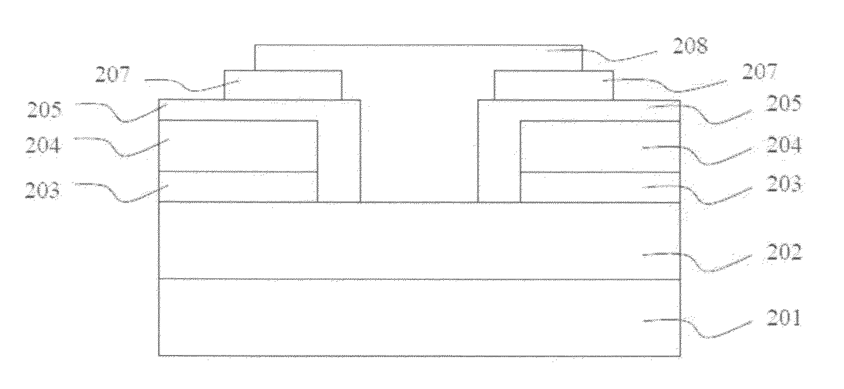
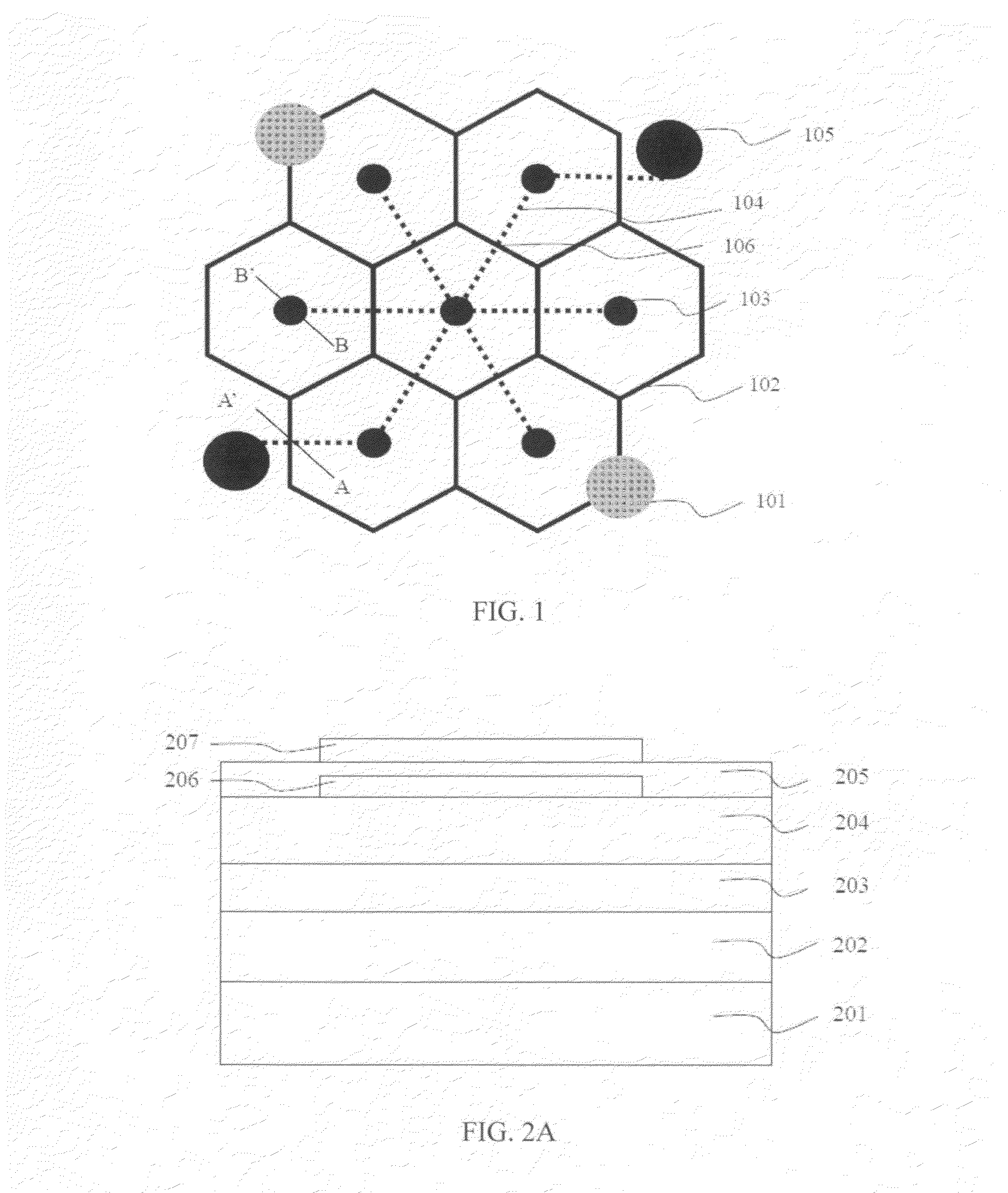
[0020]FIG. 1 shows a top view of the electrode structure of the optoelectronic semiconductor device in accordance with the present application. The device includes at least a p-type bonding pad 101, a plurality of p-type extension electrodes 102, a plurality of n-type contact zones 103, a plurality of n-type extension electrodes 104 and at least an n-type bonding pad 105. The p-type extension electrodes 102 form a plurality of symmetrical closed patterns, and at least a p-type bonding pad 101 is formed on the p-type extension electrodes 102. The n-type contact zone 103 is disposed in the symmetrical closed pattern mentioned above and electrically connected to the plurality of n-type extension electrodes 104. Besides, the p-type extension electrodes 102 and the n-type extension electrodes 104 are electrically connected to the p-type bonding pad 101 and the n-type bonding pad 105 respectively. In this embodiment, the p-type extension electrodes 102 and the n-type extension electrodes ...

fourth embodiment

[0033]FIG. 5 and FIG. 6 illustrate another layout of the electrode structure of the optoelectronic semiconductor device of the present application. FIG. 5 illustrates a top view of the layout of the electrode structure of the optoelectronic semiconductor device in accordance with the present application. The device shown in the drawing including at least one p-type bonding pad 501, a plurality of p-type extension electrodes 502, a plurality of n-type extension electrodes 503, at least an n-type bonding pad 504 and a plurality of insulating layers 505.

[0034]The p-type extension electrode 502 including a plurality of perpendicular p-type extension electrodes 5021 and a plurality of lateral p-type extension electrodes 5022 to form a plurality of symmetrical closed patterns. A plurality of straight n-type extension electrodes 5031 and a plurality of lateral n-type extension electrodes 5032 are formed in the p-type extension electrodes 502 wherein part of the perpendicular p-type extensi...

fifth embodiment

[0038]FIG. 6 illustrates a top view of the layout of the electrode structure of the optoelectronic semiconductor device in accordance with the present application. The embodiment includes at least one p-type bonding pad 601, a plurality of p-type extension electrodes 602, a plurality of n-type extension electrodes 603, at least one n-type bonding pad 604 and at least one lateral insulating layer 605.

[0039]The p-type extension electrode 602 forms a plurality of symmetrical closed patterns including a plurality of perpendicular p-type extension electrodes 6021 and a plurality of lateral p-type extension electrodes 6022. A plurality of perpendicular n-type extension electrodes 6031 and a plurality of lateral n-type extension electrodes 6032 are formed in the p-type extension electrode 602 wherein partial of the perpendicular p-type extension electrode 6021 and the lateral n-type extension electrode 6032 form the three-dimensional crossover. At least one p-type bonding pad 601 is formed...


PUM


Abstract

An optoelectronic semiconductor device includes a substrate, a semiconductor system having an active layer formed on the substrate and an electrode structure formed on the semiconductor system, wherein the layout of the electrode structure having at least a first conductivity type contact zone or a first conductivity type bonding pad, a second conductivity type bonding pad, a first conductivity type extension electrode, and a second conductivity type extension electrode wherein the first conductivity type extension electrode and the second conductivity type extension electrode have three-dimensional crossover, and partial of the first conductivity type extension electrode and the first conductivity type contact zone or the first conductivity type bonding pad are on the opposite sides of the active layer.

Description

BACKGROUND[0001]1. Technical Field[0002]An optoelectronic semiconductor device is disclosed, especially related to a layout of an electrode structure of the optoelectronic semiconductor device.[0003]2. Reference to Related Application[0004]This application claims the right of priority based on TW application Ser. No. 097146075, filed Nov. 26, 2008, entitled “OPTOELECTRONIC SEMICONDUCTOR DEVICE”, and the contents of which are incorporated herein by reference.[0005]3. Description of the Related Art[0006]The current crowding effect refers to an uneven distribution of current density occurred commonly in conventional light emitting devices. It accumulates heat locally in the lighting device and decreases the lighting efficiency. For the worse case, it damages the lighting device.[0007]The layout of the electrode structure of the light emitting device is for the purpose of spreading the current driving into the semiconductor layer more evenly and solving the issue of current crowing. The...

Claims


Application Information

Patent Timeline
Patent Type & Authority Applications(United States)
IPC IPC(8): H01L23/482
CPCH01L2924/01078H01L2924/01079Y02E10/50H01L33/382H01L31/022408H01L31/022433H01L33/38H01L24/02H01L24/05H01L24/06H01L2924/12041H01L2924/12042H01L2924/12044H01L2924/00
Inventor CHEN, WEI-YOCHEN, YEN-WENWANG, CHIEN-YUANHSIEH, MIN-HSUNCHEN, TZER-PERNG
Owner EPISTAR CORP
Why Eureka
Try Eureka