Display device,it's driving circuit, and driving method

a technology of pixel electrode and driving circuit, applied in the field of pixel electrode, can solve the problems of increasing the cost of the semiconductors as the voltage of the pixel electrode increases, and achieve the effects of reducing power consumption, reducing the amplitude of the voltage, and efficiently increasing the voltage of the pixel electrod

Active Publication Date: 2010-05-27
SHARP KK
View PDF11 Cites 9 Cited by
  • Summary
  • Abstract
  • Description
  • Claims
  • Application Information

AI Technical Summary

Benefits of technology

[0051]According to the first aspect of the present invention, a period in which each scanning signal line is selected (scanning signal line selection period) includes a first selection period and a second selection period, as described below. During the first selection period, all switching elements included in a row corresponding to a selected scanning signal line (hereinafter, referred to as a “selected row”) are rendered conductive. As a result, a voltage applied to the video signal line is supplied to all pixel electrodes included in the selected row. Also, during a period between the first selection period and the second selection period, potentials of predetermined electrodes capacitively coupled to the pixel electrodes included in the selected row are changed. As a result, potentials of all pixel electrodes included in the selected row are changed in accordance with the change of the potentials of the predetermined electrodes. Furthermore, during the second selection period, apart of the switching elements included in the selected row are rendered conductive. In this case, any switching element corresponding to a pixel electrode that should be subjected to writing of a tone value within a first gradation range is rendered non-conductive, and therefore, the voltage of the pixel electrode is maintained at a level at the start point of the second selection period. On the other hand, any pixel electrode that should be subjected to writing of a tone value outside the first gradation range is supplied with a voltage corresponding to that tone value. Accordingly, the amplitude of the pixel electrode voltage is set greater than the amplitude of the voltage supplied to the video signal line by an amount of change (in the pixel electrode potential) in accordance with the change of the potential of the predetermined electrode. Thus, it is possible to employ display elements with a relatively large difference between the minimum tone voltage and the maximum tone voltage, without changing the conventional amplitude of the voltage to be provided to the video signal line. Also, in the case where display elements with the same difference between the minimum tone voltage and the maximum tone voltage as conventional are used, it is possible to reduce the amplitude of the voltage to be provided to the video signal line below the conventional amplitude, thereby reducing power consumption.
[0052]According to the second aspect of the present invention, at the start point of the second selection period, to a pixel electrode that should be subjected to writing of a tone value within a first gradation range, a voltage corresponding to each tone value is provided. In addition, the voltage corresponds to a voltage at which the switching element is rendered non-conductive, and therefore the pixel electrode voltage is maintained during the second selection period. Thus, it is possible, without impairing a gradation display based on a tone signal indicating a tone value within the first gradation range, to shift the pixel electrode voltage, thereby setting the amplitude thereof greater than the amplitude of the voltage provided to the video signal line.
[0053]According to the third aspect of the present invention, as for all switching elements corresponding to pixel electrodes that are provided with the same second voltage during the first selection period and should be subjected to writing of a tone value within the second gradation range, they are rendered conductive during the second selection period. Here, tone values within the first gradation ranges and tone values within the second gradation ranges are exclusive to each other, and any tone signal indicating a tone value outside the first gradation range is converted into a voltage corresponding to each tone value during the second selection period. Accordingly, any tone signal indicating a tone value within the second gradation range is also converted into a voltage corresponding to each tone value during the second selection period. On the other hand, as for all switching elements corresponding to pixel electrodes that should be subjected to writing of a tone value within the first gradation range, they are rendered non-conductive during the second selection period. Thus, it is possible to set the amplitude of the pixel electrode voltage greater than the amplitude of the voltage provided to the video signal line, without impairing a gradation display based on a tone signal indicating a tone value within the first gradation range.
[0054]According to the fourth aspect of the present invention, the maximum possible amplitude of the pixel electrode voltage is a sum of an amplitude corresponding to the difference between the minimum value and the maximum value of a voltage that can be applied to the video signal line and an amplitude corresponding to an amount of change (in the pixel electrode potential) in accordance with the change of the potential of the predetermined electrode. Thus, it is possible to efficiently increase the amplitude of the pixel electrode voltage.
[0055]According to the fifth aspect of the present invention, all switching elements included in a selected row are rendered non-conductive during a period between the first selection period and the second selection period. As a result, all pixel electrodes included in the selected row are each electrically isolated from the video signal line in accordance with the change of the potential of the predetermined electrode, making it possible to reliably change the potential thereof.
[0056]According to the sixth aspect of the present invention, the potential of the pixel electrode can be changed by changing the potential of the common electrode. Thus, it is possible to increase the amplitude of the pixel electrode voltage with a relatively simple configuration.

Problems solved by technology

Semiconductors increase in cost as their withstanding voltage increases.

Method used


Image

  • Display device,it's driving circuit, and driving method
  • Display device,it's driving circuit, and driving method
  • Display device,it's driving circuit, and driving method

Examples


first embodiment

2. First Embodiment

2.1 Overall Configuration and Operation

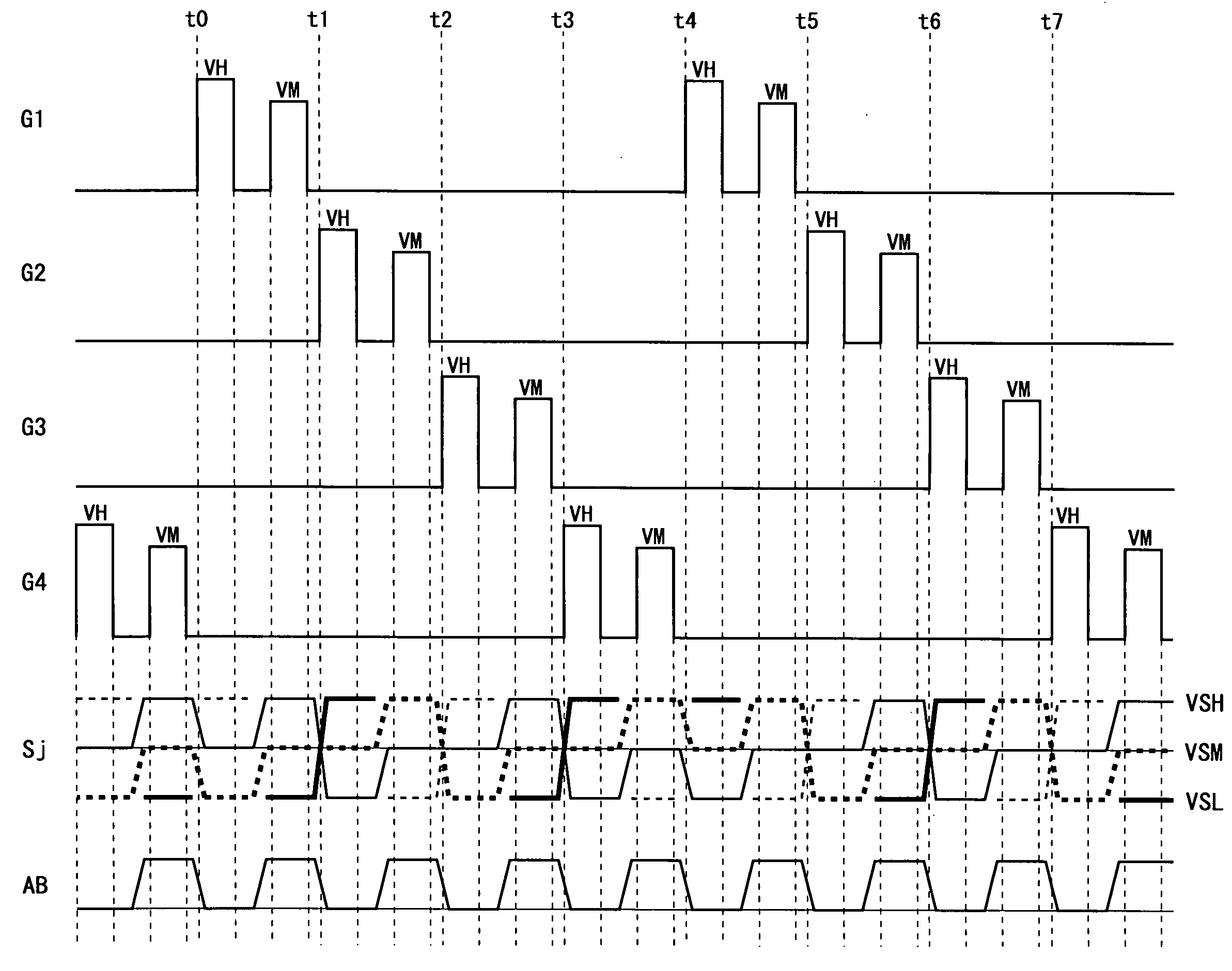
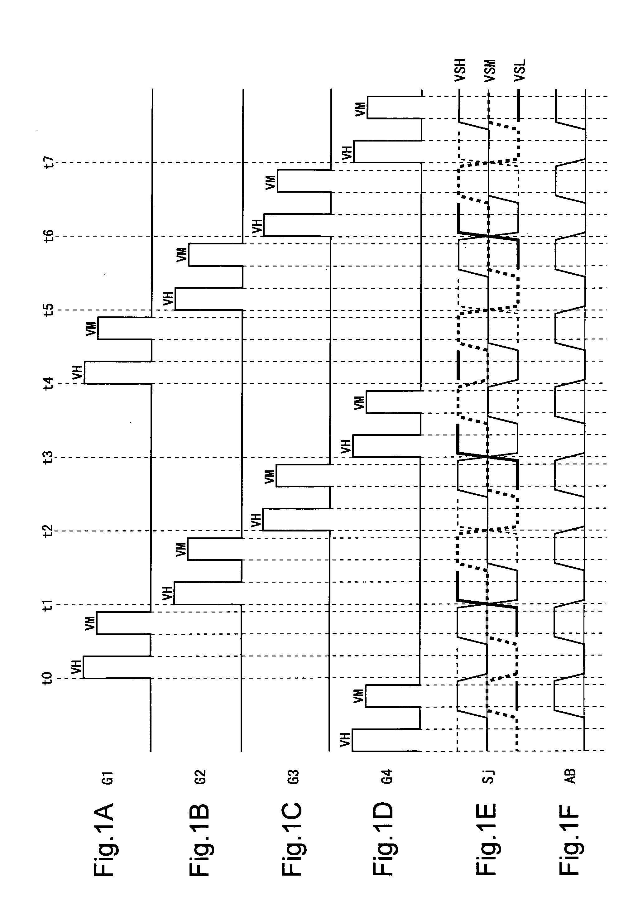
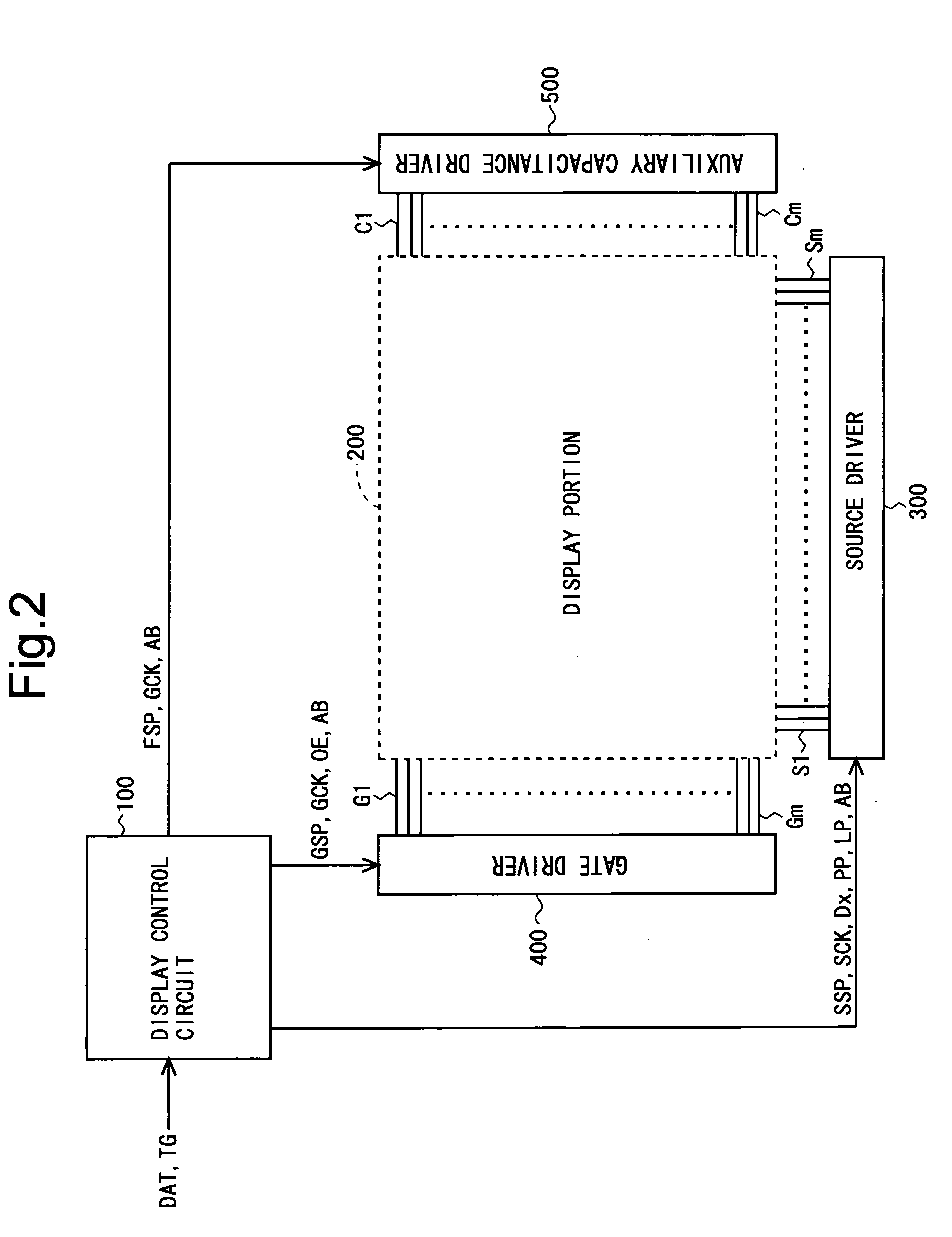
[0132]FIG. 2 is a block diagram illustrating the overall configuration of a liquid crystal display device according to a first embodiment of the present invention. The liquid crystal display device includes a display control circuit 100, a display portion 200, a source driver (video signal line drive circuit) 300, a gate driver (scanning signal line drive circuit) 400, and an auxiliary capacitance driver (auxiliary capacitance electrode drive circuit) 500. Hereinafter, the source driver 300, the gate driver 400, and the auxiliary capacitance driver 500 may also be collectively referred to as a driver (drive circuit). FIG. 3 is a block diagram illustrating detailed configurations of the drivers and the display portion 200 in the liquid crystal display device. Note that the liquid crystal display device performs a 64-tone gradation display.

[0133]The display portion 200 includes n source lines (video signal lines) S1 to Sn, m ga...

second embodiment

3. Second Embodiment

[0181]FIG. 15 is a block diagram illustrating configurations of drivers and a display portion 200 in a liquid crystal display device according to a second embodiment of the present invention. In the present embodiment, unlike in the first embodiment, all auxiliary capacitance lines Ck are electrically connected to the common electrode 24. Accordingly, no auxiliary capacitance driver 500 is provided.

[0182]FIGS. 16A to 16D are signal waveform diagrams describing a drive method in the present embodiment. In the present embodiment, since all auxiliary capacitance lines Ck are electrically connected to the common electrode 24, as described above, the voltage of the common electrode 24 and the voltages of the auxiliary capacitance lines Ck change in the same manner, as shown in FIG. 16C. Note that as in the first embodiment, the waveform of the selection signal applied to the gate line G1, the waveform of the drive video signal applied to the source line Sj, and the wa...

third embodiment

4. Third Embodiment

[0197]FIG. 17 is a block diagram illustrating configurations of drivers and a display portion 200 in a liquid crystal display device according to a third embodiment of the present invention. In the present embodiment, the auxiliary capacitance lines are divided into four groups. Note that, in the example shown in FIG. 17, there are four auxiliary capacitance lines, and therefore each group includes only one auxiliary capacitance line, but in the case where there are, for example, 240 auxiliary capacitance lines, each group includes 60 auxiliary capacitance lines. In the present embodiment, when grouping the auxiliary capacitance lines, they are initially divided into overlying groups and underlying groups with respect to the center of the display portion 200, and further divided into groups of odd-numbered rows and even-numbered rows. For example, when there are 240 auxiliary capacitance lines, the auxiliary capacitance lines in the “first row, third row, fifth ro...


PUM


Abstract

One embodiment of the present invention discloses a display device which can use a display element having a relatively large difference between a minimum gradation voltage and a maximum gradation voltage. A first selection period and a second selection period are included in a period (a scanning signal line selection period) in which each gate wiring is selected. In the first selection period, a first selection voltage for allowing every TFT included in a line, which is an object to be selected, to be in an ON state is applied to the gate wiring of the line which is the object to be selected. In a period between the first selection period and the second selection period, a non selection voltage is applied to the gate wiring which is the object to be selected and the voltage of an auxiliary capacity wiring corresponding to the gate wiring which is the object to be selected is changed. In the second selection period, a second selection voltage for allowing a part of the TFTs included in the line, which is the object to be selected, to be in an ON state is applied to the gate wiring which is the object to be selected.

Description

TECHNICAL FIELD[0001]The present invention relates to display devices, such as liquid crystal display devices, and particularly to a display device with reduced power consumption and improved response speed, as well as to a circuit and method for driving the same.BACKGROUND ART[0002]In recent years, liquid crystal display devices using TFTs (Thin Film Transistors), as in notebook computers, cell phones, and liquid crystal televisions, have become widespread. In liquid crystal display devices using TFTs, a drive circuit called a “source driver” supplies voltage to a liquid crystal in order to control the state of display by the liquid crystal. The source driver is configured by a semiconductor such as an IC (Integrated Circuit). Semiconductors increase in cost as their withstanding voltage increases. Therefore, the cost of liquid crystal display devices is reduced by narrowing the amplitude of an output voltage from the source driver.[0003]For example, Japanese Laid-Open Patent Publi...

Claims


Application Information

Patent Timeline
Patent Type & Authority Applications(United States)
IPC IPC(8): G06F3/038
CPCG09G2330/021G09G3/3659
Inventor NUMAO, TAKAJI
Owner SHARP KK
Why Eureka
Try Eureka