Pipe latch circuit and driving method thereof

a latch circuit and circuit technology, applied in the field of semiconductor design technology, can solve the problems of reducing the valid data window, reducing the accuracy of data output, and reducing the number of valid data windows, so as to minimize the number of control signals, minimize the skew generated while data is transferred, and minimize the effect of skew

Active Publication Date: 2010-06-10
SK HYNIX INC
View PDF6 Cites 14 Cited by
  • Summary
  • Abstract
  • Description
  • Claims
  • Application Information

AI Technical Summary

Benefits of technology

[0046]A pipe latch circuit and a driving method thereof according to embodiments of the present invention minimize the number of control signals responding a synchronization signal among the control signals in the pipe latch circuit. Therefore, a skew generated while the data is transferred can be minimized. Particularly, the skew can be minimized and a valid data window can be maximized by using information for deciding an output order of a plurality of data to a clock signal for controlling the final outputting of the pipe latch circuit. Furthermore, data with a stable valid data window can improve a margin with a control signal of an output driver for driving an input / output pad.

Problems solved by technology

The high operation frequency may cause problems that were not generated in a semiconductor memory device having a comparatively low operation frequency.
As an example of the problems, a data margin problem of data that is synchronized with a clock signal corresponding to the operation frequency has been receiving attention.
Such a problem similarly occurs when the falling pipe latch unit 110F outputs the falling output signal FDOB, and reduces a valid data window of the rising output signal RDOB and the falling output signal FDOB.
Finally, such a margin problem may cause an error that makes the semiconductor memory device to inaccurately output data.

Method used


Image

  • Pipe latch circuit and driving method thereof
  • Pipe latch circuit and driving method thereof
  • Pipe latch circuit and driving method thereof

Examples


Embodiment Construction

[0053]Other objects and advantages of the present invention can be understood by the following description, and become apparent with reference to the embodiments of the present invention.

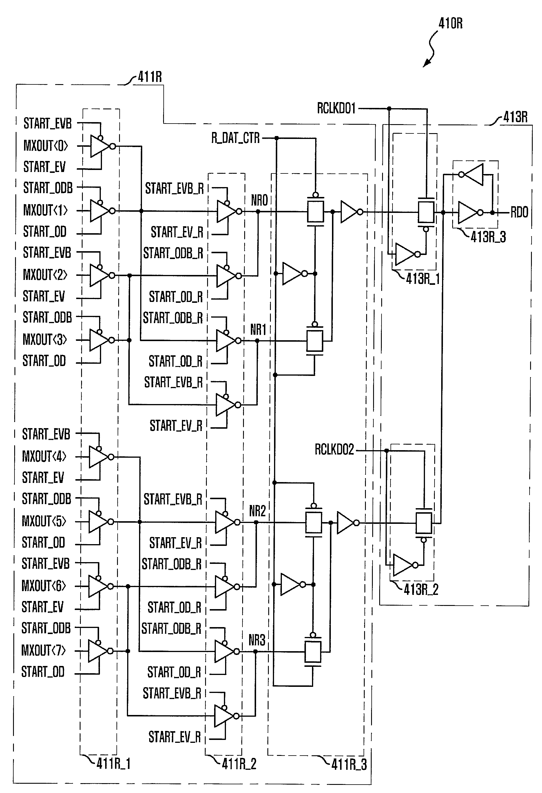
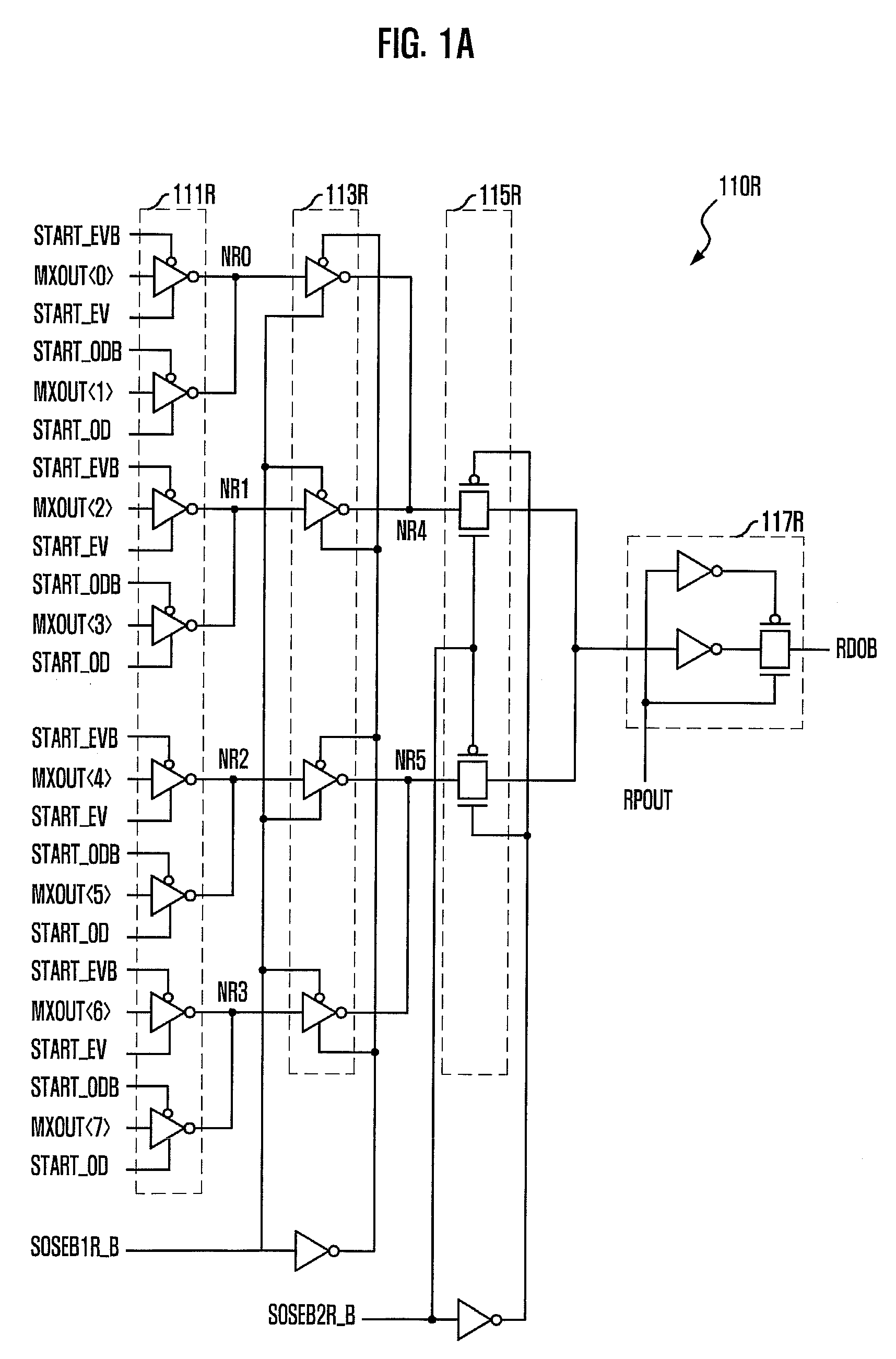
[0054]FIGS. 4A and 4B are circuit diagrams illustrating a part of a pipe latch circuit in accordance with an embodiment of the present invention.

[0055]The pipe latch circuit according to the present embodiment includes a rising pipe latch unit 410R corresponding to a rising edge of a DLL clock signal, which is shown in FIG. 4A, and a falling pipe latch unit 410F corresponding to a falling edge of a DLL clock signal, which is shown in FIG. 4B.

[0056]Referring to FIG. 4A, the rising pipe latch unit 410R receives zeroth to seventh data MXOUT and outputs a rising output signal RDO in an order corresponding to address information in response to first and second rising clock signals RCLKDO1 and RCLKDO2. The rising pipe latch unit 410 includes a rising pipe input unit 411R and a rising pipe output unit 413R...


PUM


Abstract

A pipe latch circuit includes a pipe input unit configured to receive a plurality of data in an order corresponding to address information, a control signal generator configured to generate first and second control clock signals by using the address information, where the first and second control clock signals correspond to a synchronization clock signal, and a pipe output unit configured to synchronize an output signal of the pipe input unit with the first and second control clock signals and output the synchronized output signal.

Description

CROSS-REFERENCE(S) TO RELATED APPLICATIONS[0001]The present invention claims priority of Korean patent application number 10-2008-0122534, filed on Dec. 4, 2008, which is incorporated by reference in its entirety.BACKGROUND OF THE INVENTION[0002]The present invention relates to a semiconductor design technology, and more particularly, to a pipe latch circuit for serializing a plurality of data in a predetermined order to output the serialized data, and a driving method thereof.[0003]A semiconductor memory device such as Double Data Rate Synchronous DRAM (DDR SDRAM) has been advanced for achieving high speed data processing and large storage capacity. A conventional semiconductor memory device such as a Single Data Rate Synchronous DRAM (SDR SDRAM) outputs a plurality of data by synchronizing the data with a rising edge of an external clock signal. However, the semiconductor memory device such as a DDR SDRAM outputs a plurality of data by synchronizing the data not only with a rising...

Claims


Application Information

Patent Timeline
Patent Type & Authority Applications(United States)
IPC IPC(8): G11C8/16
CPCG11C7/1018G11C7/103H03K3/012G11C7/106G11C7/1066G11C7/1051G11C11/4093G11C11/4096G11C11/4076
Inventor KIM, JAE-IL
Owner SK HYNIX INC
Why Eureka
Try Eureka