Circuit substrate and circuit substrate manufacturing method

a manufacturing method and circuit substrate technology, applied in the direction of final product manufacturing, sustainable manufacturing/processing, semiconductor/solid-state device details, etc., can solve the problems of poor connection between circuit substrate and ic, difficult to accurately mount the ic on the circuit substrate, and heat damage to the circuit substra

Active Publication Date: 2010-06-17
MURATA MFG CO LTD
View PDF14 Cites 4 Cited by
  • Summary
  • Abstract
  • Description
  • Claims
  • Application Information

AI Technical Summary

Benefits of technology

[0024]According to a preferred embodiment of the present invention, the top surface of the terminal is wider than the section of the terminal on the moun

Problems solved by technology

However, when performing the above-mentioned mounting method, for example, the circuit substrate may become distorted by heat, since the thermal expansion coefficient of the circuit substrate is different from that of the IC.
Thu

Method used


Image

  • Circuit substrate and circuit substrate manufacturing method
  • Circuit substrate and circuit substrate manufacturing method
  • Circuit substrate and circuit substrate manufacturing method

Examples


Embodiment Construction

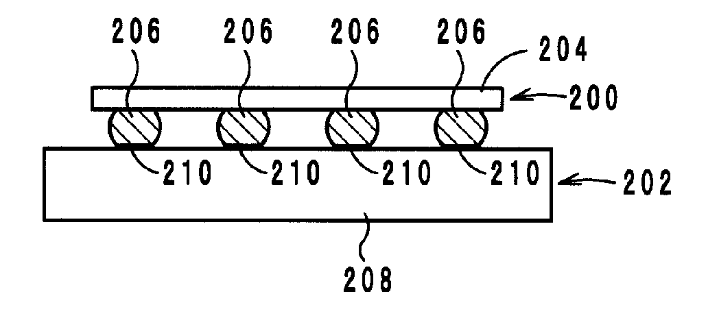
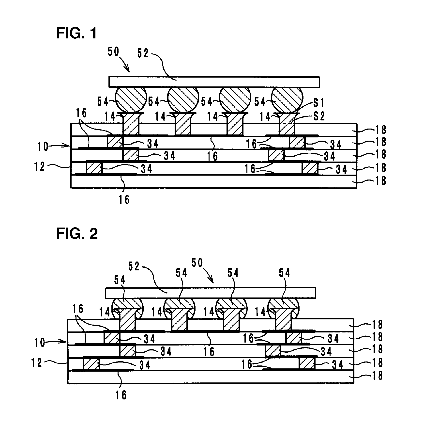
[0037]A configuration of a circuit substrate will be described below with reference to the drawings. FIG. 1 is a sectional structure drawing showing a state where a semiconductor integrated circuit (hereafter referred to as an “IC”) 50 is aligned with a circuit substrate 10. FIG. 2 is a drawing showing a sectional structure after reflow is performed on the IC 50 and circuit substrate 10 shown in FIG. 1.

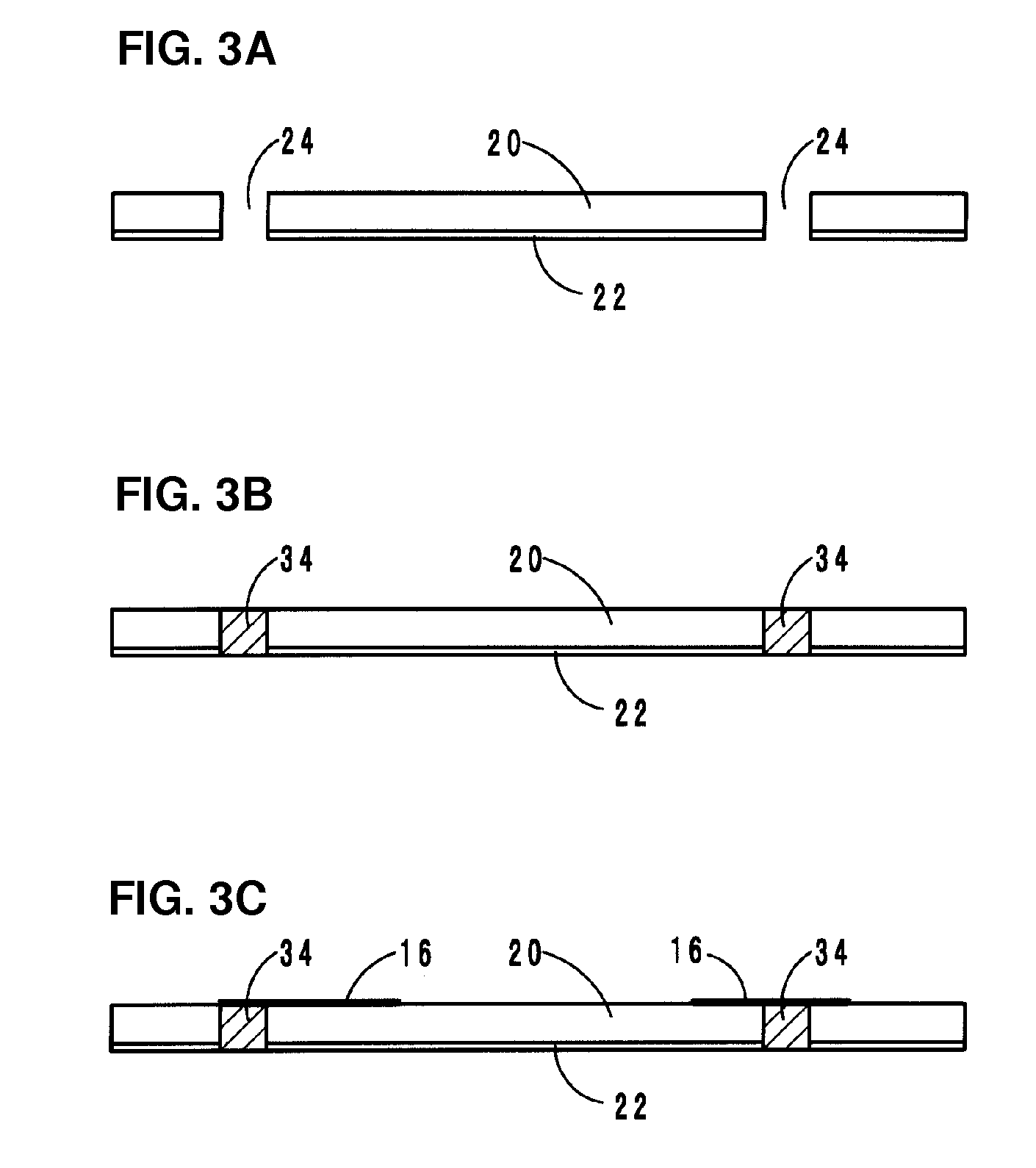
[0038]The circuit substrate 10 is a substrate on which the IC 50, which is an electronic component, is to be surface-mounted. As shown in FIG. 1, the circuit substrate 10 includes a substrate body 12, terminal 14, and internal conductive layers 16. The substrate body 12 is preferably formed by laminating multiple ceramic layers 18, which are insulators. The internal conductive layers 16 are laminated together with the ceramic layers 18 inside the substrate body 12 so as to form a circuit. The internal conductive layers 16 are connected to one another through via conductors 34.

[0039]Th...


PUM

PropertyMeasurementUnit
Temperatureaaaaaaaaaa

Abstract

A circuit substrate includes protruding terminals and has a structure that ensures an excellent connection with an electronic component, such as an IC. The circuit substrate on which an IC is to be mounted includes terminals that are to be electrically connected to solder bumps located on the IC. The terminals protrude from the mounting surface of a substrate body on which the IC is to be mounted. The sectional area of the top surface of each of the terminals is about 1.2 times the sectional area of each of the terminals on the mounting surface.

Description

BACKGROUND OF THE INVENTION[0001]1. Field of the Invention[0002]The present invention relates to a circuit substrate and a circuit substrate manufacturing method and, in particular, to a circuit substrate on which an electronic component is to be mounted and a circuit substrate manufacturing method.[0003]2. Description of the Related Art[0004]Conventionally, when mounting an electronic component, such as an IC, on a circuit substrate, a mounting method as described below has been performed. Flat electrode pads are formed in an array on the main surface of the circuit substrate. On the other hand, solder bumps are formed in an array on the main surface of the IC. The IC is placed on the circuit substrate in such a manner that the solder bumps are positioned on the electrode pads, and then reflow is performed. Thus, the solder bumps are molten and then the solder bumps and electrode pads are fixed to each other. In this way, the IC is mounted on the circuit substrate.[0005]However, wh...

Claims


Application Information

Patent Timeline
IPC IPC(8): H05K1/00H05K1/11H05K3/30H05K3/40
CPCH01L23/49816Y10T29/49155H01L24/16H01L24/81H01L2224/11003H01L2224/16H01L2224/81193H01L2224/81801H01L2924/01004H01L2924/14H05K1/0306H05K1/111H05K3/245H05K3/3436H05K3/4007H05K3/4061H05K3/4611H05K3/4629H05K2201/0367H05K2203/0191H05K2203/0278H05K2203/308H01L23/49827Y10T29/4913H01L2224/81143H01L2224/131H01L2924/00011H01L2924/00014H01L2924/12042Y02P70/50H01L2924/00H01L2224/0401
Inventor FUKUDA, YUTAKA
Owner MURATA MFG CO LTD
Why Eureka
Try Eureka