Ceramic capacitor

a ceramic capacitor and capacitor technology, applied in the field of ceramic capacitors, can solve the problems of ceramic capacitors undergoing decreases in strength, generating breakage or cracks, etc., and achieve the effects of improving degree of freedom, reducing or preventing defective connections, and increasing area

Active Publication Date: 2017-11-30
MURATA MFG CO LTD
View PDF2 Cites 5 Cited by
  • Summary
  • Abstract
  • Description
  • Claims
  • Application Information

AI Technical Summary

Benefits of technology

[0084]It is to be noted that the respective lengths of the first and second portions 15a, 15b of the first external electrode 15, and of the fifth and sixth portions 16a, 16b of the second external electrode 16 in the laminating direction T can be obtained by observing the end surfaces of the ceramic capacitor with the use of a metallograph, and measuring the maximum lengths in the laminating direction T.
[0085]The respective lengths of the third and fourth portions 15c, 15d of the first external electrode 15, and of the seventh and eighth portions 16c, 16d of the second external electrode 16 in the laminating direction T can be obtained by observing the end surfaces of the ceramic capacitor with the use of a metallograph, and measuring the maximum lengths in the width direction W.
[0086]The respective lengths of the first, second, fifth, and sixth portions 15a, 15b, 16a, 16b in the laminating direction T are preferably smaller than the lengths of the third, fourth, seventh, and eighth portions 15c, 15d, 16c, 16d in the width direction. In this case, it becomes possible to reduce not only the first, second, fifth, and sixth portions 15a, 15b, 16a, 16b, but also the external electrodes 15, 16 in thickness in the laminating direction T, thus making the ceramic capacitor 1 thinner. Therefore, the ceramic capacitor 1 is able to be made more suitable for mounting onto a built-in electronic component substrate.
[0087]In the ceramic capacitor 1 according to the present preferred embodiment, when the lengths of the portions of the third external electrode 17 located on the first and second principal surfaces 10a, 10b in the length direction L are denoted by A, whereas the lengths of the portions of the third external electrode 17 located on the first and second side surfaces 10c, 10d in the length direction L are denoted by B, the magnitude relationship A>B is satisfied. According to this configuration, the areas of the portions of the third external electrode 17 located on the first and second principal surfaces 10a, 10b are able to be increased. For this reason, the area is able to be increased which is irradiated with laser light to form a via hole leading to the third external electrode 17 of the ceramic capacitor 1 in a substrate with the ceramic capacitor 1 embedded therein. Accordingly, defective connections are able to be significantly reduced or prevented between the via hole electrode and the ceramic capacitor 1. In addition, the degree of freedom is improved for the location of the via hole electrode.
[0088]In addition, the magnitude relationship of A>B increases the area of exposure, from the external electrodes 15 to 17, of the side surfaces 10c, 10d of the capacitor main body 10 which has higher adhesion to the substrate than the surface of the external electrode 17. Therefore, the area of contact is able to be increased between the side surfaces 10c, 10d and the resin of the substrate. Accordingly, the adhesion between the substrate and the ceramic capacitor 1 is able to be improved. As a result, migration is effectively prevented from being caused by ingress of water from between the substrate and the ceramic capacitor.
[0089]From the perspective of preventing defective connection between via hole electrodes and the ceramic capacitor 1 in a more effective manner, and from the perspective of further improving the adhesion between the substrate and the ceramic capacitor 1, thus preventing migration in a more effective manner, the ratio B / A is preferably about 0.96 or less, for example.

Problems solved by technology

Therefore, the decreased height dimensions of the ceramic capacitors have a tendency to cause the ceramic capacitors to undergo decreases in strength.
Accordingly, problems such as generation of breakage or cracks may be developed with the ceramic capacitors.

Method used


Image

  • Ceramic capacitor
  • Ceramic capacitor
  • Ceramic capacitor

Examples


examples 1 to 3

[0109]With the use of the manufacturing method described with reference to the preferred embodiments mentioned above, 1000 capacitors configured in substantially the same fashion as the ceramic capacitors 1 according to the preferred embodiments were prepared under the following conditions.

Conditions:

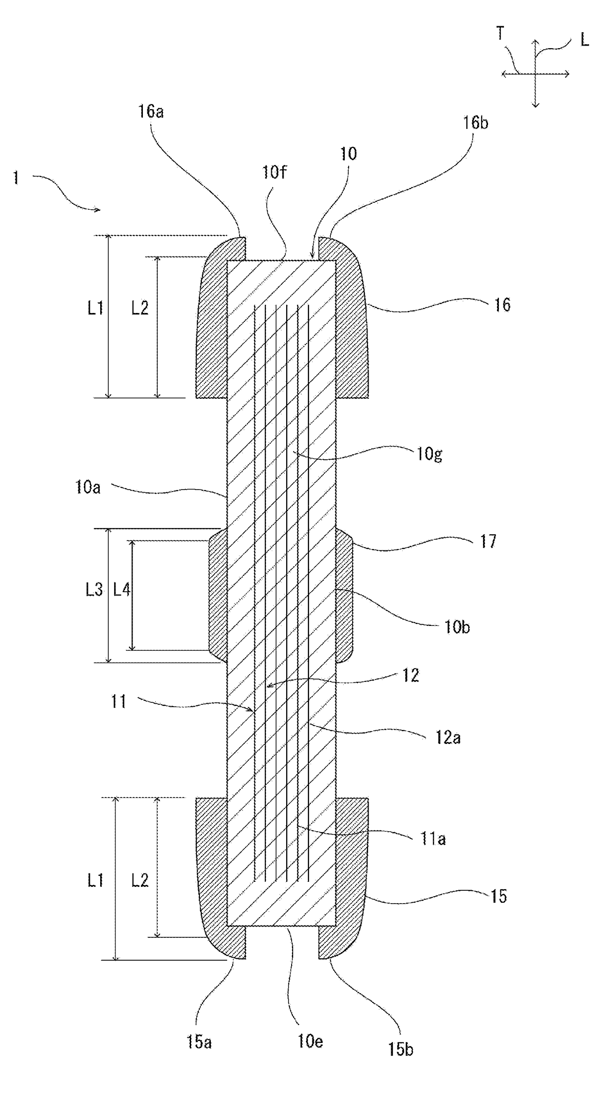
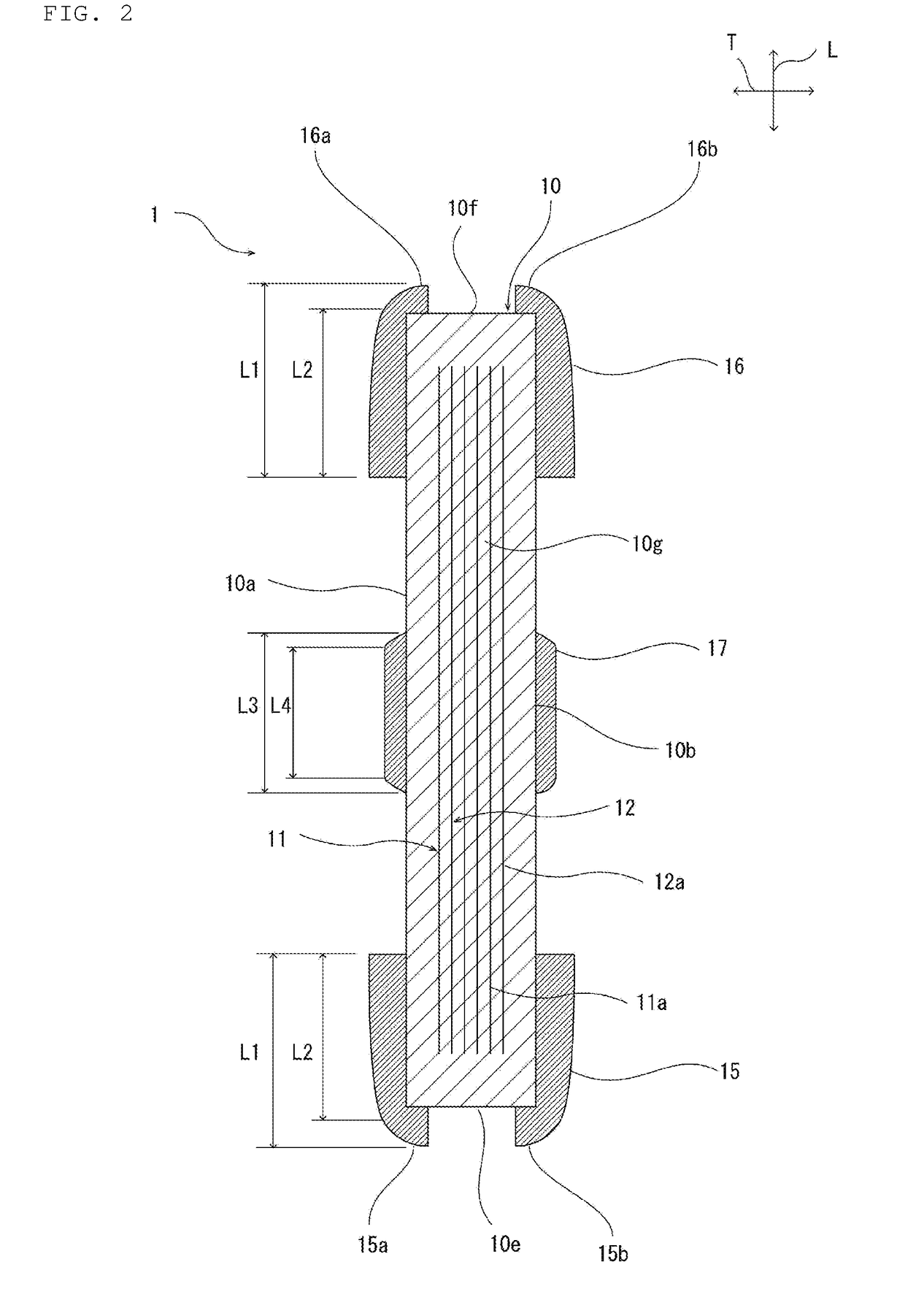
[0110]Dimensions of Ceramic Capacitor (Standard Dimension):L×W×T=1.000 mm×0.600 mm×0.220 mm

[0111]Ceramic Material: BaTi2O3

[0112]Capacitance: 1 μF

[0113]Rated Voltage: 6.3 V

[0114]Structure of External Electrode: Base Electrode Layer / Thin Film Electrode Layer / Plated Layer

[0115]Base Electrode Layer: Ni Fired Electrode Layer

[0116]Thin Film Electrode Layer: NiCr Sputtering Film / NiCu Sputtering Film

[0117]Plated Layer: Single Cu Plated Layer

[0118]Thickness of Base Electrode Layer (Central Part): 6 μm

[0119]Thickness of Thin Film Electrode Layer (Central Part):0.3 μm in total (0.15 μm for each layer)

[0120]Thickness of Plated Layer (Central Part): 10 μm


PUM

PropertyMeasurementUnit
thicknessaaaaaaaaaa
thicknessaaaaaaaaaa
thicknessaaaaaaaaaa

Abstract

In a planar view of a ceramic capacitor that has low ESL and is embeddable into a substrate, lengths of first and second external electrodes are L1, lengths from portions of the first and second external electrodes farthest from a capacitor main body to portions closer to the capacitor main body by about 40% of a thickness of the first or second external electrode in a laminating direction are L2, a ratio L2/L1 is about 80% or more and about 90% or less. In the planar view, a length of a third external electrode is L3, a length from a portion of the third external electrode farthest from the capacitor main body to a portion closer to the capacitor main body by about 40% of a thickness of the third external electrode in the laminating direction is L4, a ratio L4/L3 is about 80% or more.

Description

CROSS REFERENCE TO RELATED APPLICATIONS[0001]This application claims the benefit of priority to Japanese Patent Application No. 2016-108585 filed on May 31, 2016. The entire contents of this application are hereby incorporated herein by reference.BACKGROUND OF THE INVENTION1. Field of the Invention[0002]The present invention relates to a ceramic capacitor.2. Description of the Related Art[0003]In recent years, information terminal devices such as cellular phones and portable music players have been progressively reduced in size and made thinner. Accordingly, substrates to be mounted in electronic devices and electronic components to be mounted on substrates have been also progressively reduced in size. Electronic components to be mounted on substrates have been also progressively mounted at higher density. In order to achieve further reduction in size for electronic components, built-in electronic component substrates with electronic components embedded in the substrates have been a...

Claims


Application Information

Patent Timeline
Patent Type & Authority Applications(United States)
IPC IPC(8): H01G4/12H01G4/005H01G4/30C23C14/34
CPCH01G4/1209H01G4/302C23C14/34H01G4/005H01G4/306H01G4/232
Inventor USUI, KAZUNORI
Owner MURATA MFG CO LTD
Why Eureka
Try Eureka