Adjustable integrator using a single capacitance

a capacitance and integrator technology, applied in the field of circuits and methods of integrating amplifiers, can solve the problems of a large die area, design which needs to be placed inside small packages, and the amount of charge that can be measured, so as to prevent dc offset

Inactive Publication Date: 2010-06-24
DIALOG SEMICONDUCTOR GMBH
View PDF7 Cites 3 Cited by
  • Summary
  • Abstract
  • Description
  • Claims
  • Application Information

AI Technical Summary

Benefits of technology

[0017]It is yet a further object of the present invention to prevent a DC offset in a current mirror.
[0018]These and many other objects have been achieved by coupling an output stage, comprising a current mirror, to the integrating amplifier. The output of the first current source of the current mirror is coupled via the external integrating capacitor to the input of the integrating amplifier. The output of the second current source of the current mirror, which mirrors the current of the first current source and thus the output current of the integrating amplifier, is fed back to th

Problems solved by technology

Because of the limited output swing of the amplifier the amount of the charge that can be measured is limited.
This is a disadvantage for designs which need to be placed inside small packages and where pads are either at a premium or

Method used


Image

  • Adjustable integrator using a single capacitance
  • Adjustable integrator using a single capacitance
  • Adjustable integrator using a single capacitance

Examples


Embodiment Construction

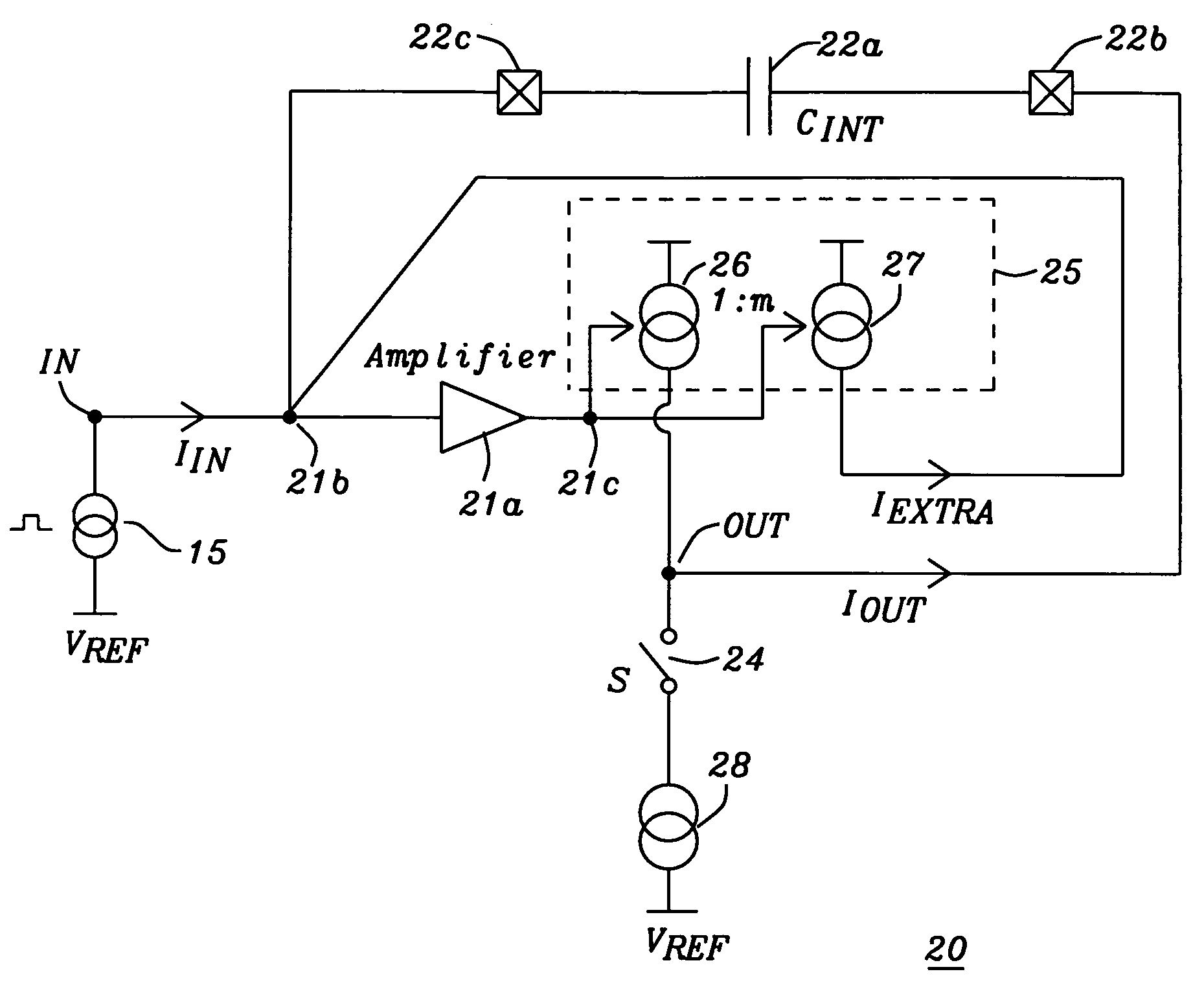
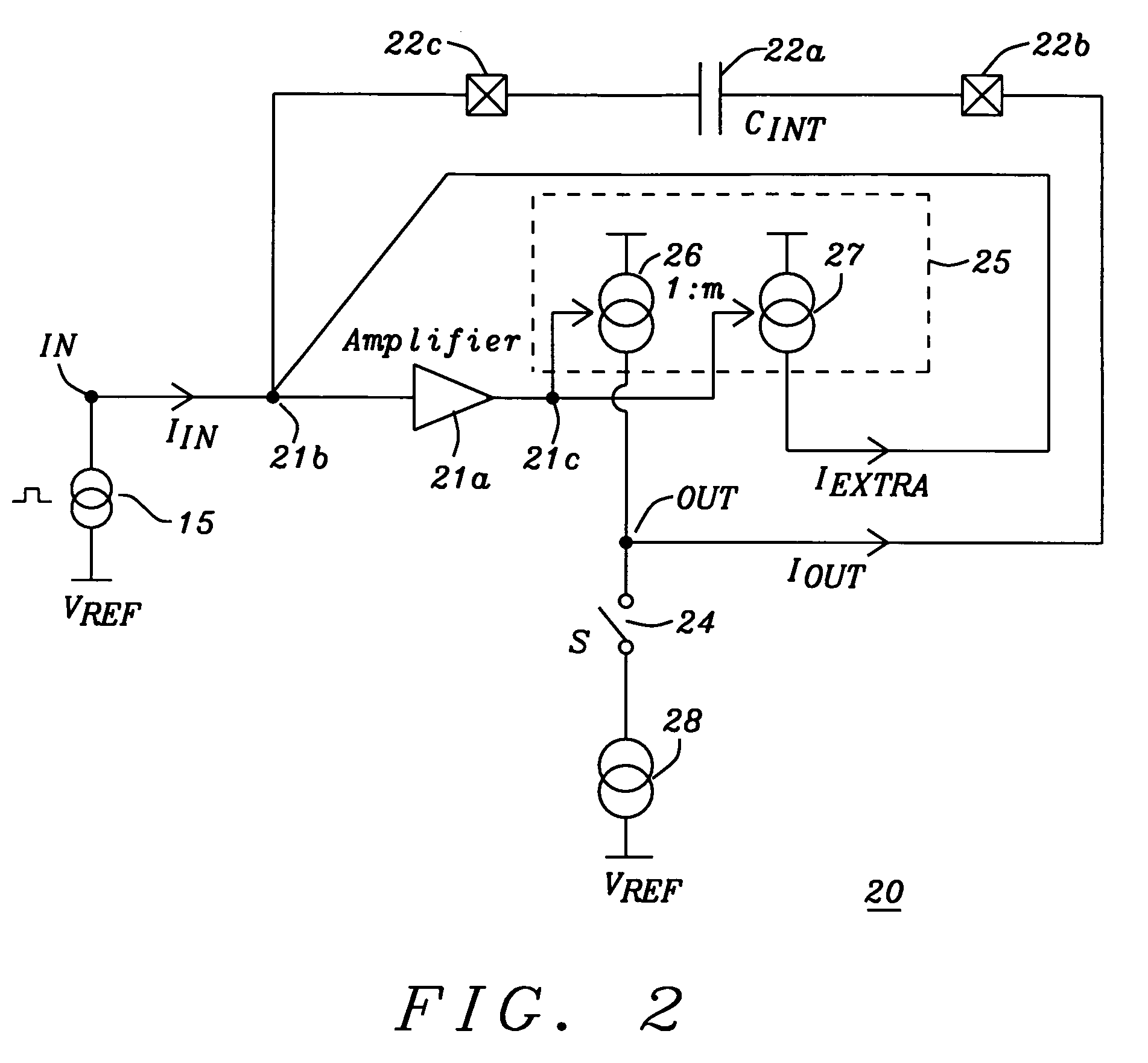
[0025]In the preferred embodiment of the present invention of an adjustable integrator, a current mirror is used in the output stage of the amplifier which feeds back a duplicate of the output current of the amplifier to its input node. This is be done on the die (chip) without requiring an extra pad. This method results in an integrator output voltage of:

VOUT=IINt(1+m)CINT

where with reference to FIG. 2:[0026]VOUT is the voltage at output OUT,[0027]IIN is the current flowing into the input of the amplifier,[0028]CINT is the integrating capacitor, and[0029]m is a factor for the current feedback replication.

[0030]Using current feedback, the range in the present invention is not limited to the voltage output range of the amplifier. The present invention utilizes only one capacitor and thus requires only two pads to handle the range switching. The extra current IEXTRA is generated by mirroring the current IOUT in the output stage of the amplifier. To avoid a DC offset in the mirrored cu...


PUM


Abstract

An integrating amplifier on an IC, which comprises a feedback loop using an external device as an integrating capacitor, has added a second feedback loop that provides an additional current to the input of the amplifier, which current can be used to increase the input range of the charge that can be measured without needing another external capacitor or pad.

Description

BACKGROUND OF THE INVENTION[0001]1. Field of the Invention[0002]The invention relates to a circuit and a method for an integrating amplifier which increases the input range of the charge that can be measured, and more particularly to an integrating amplifier on an IC where an internal feedback loop is added thereby eliminating the need for a another external capacitor and pad.[0003]2. Description of the Related Art[0004]To measure charge and thus capacitance, an amplifier wired as an integrator could be used. The charge to be measured is injected into the input of the amplifier and from there is fed, via an integrating capacitance, to the output of the amplifier. The measurement is initiated by a current pulse on the input of the integrator. The integrating capacitance, connected between the negative input and the output of the amplifier, collects the charge transferred by the input pulse. Because of the limited output swing of the amplifier the amount of the charge that can be meas...

Claims


Application Information

Patent Timeline
IPC IPC(8): G06G7/18
CPCG06G7/186
Inventor STELLBERGER, ACHIMKELLER, MICHAELZEHNICH, PAUL
Owner DIALOG SEMICONDUCTOR GMBH
Why Eureka
Try Eureka