Touch panel
Active Publication Date: 2010-06-24
GUNZE LTD
View PDF7 Cites 9 Cited by
- Summary
- Abstract
- Description
- Claims
- Application Information
AI Technical Summary
Benefits of technology
[0015]In the present invention, the gaps between all the divided electrodes are of the same shape, and the distortion of the equipotential lines can be made as little as possible by adjusting the ratio of the length of each of the divided electrodes at both ends to the length of each of the other divided electrodes. This makes it possible to reduce the distortion of the equipotential lines more easily than in the case of individually adjusting the sizes of the T-shapes of Patent Document 1.
[0016]The design is easily made by making the shapes of all the gaps substantially the same. In addition, when the electrodes are made pectinate, it is possible to prevent the electrodes other than the electrodes on the innermost side from affecting the formation of the equipotential lines.
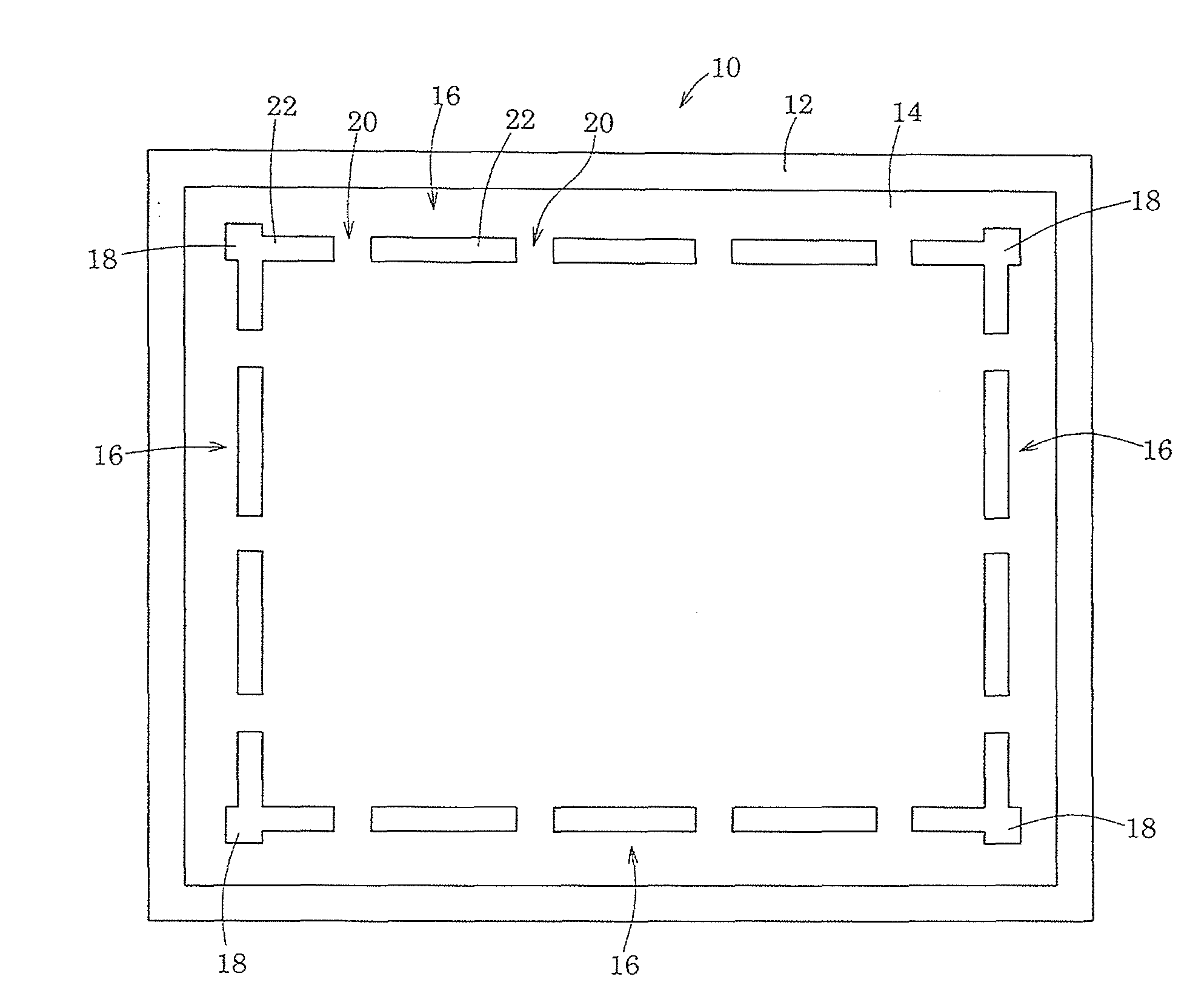
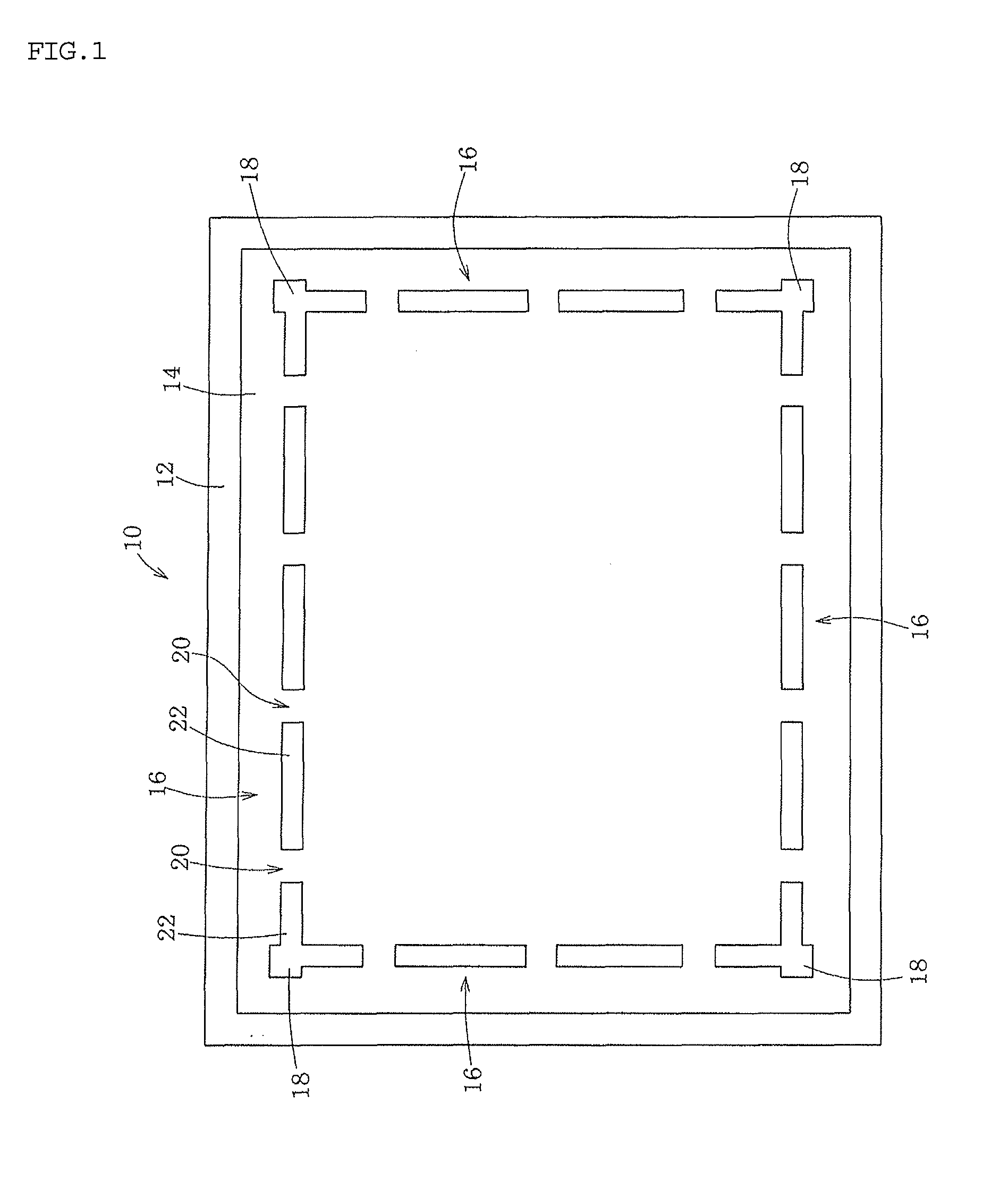
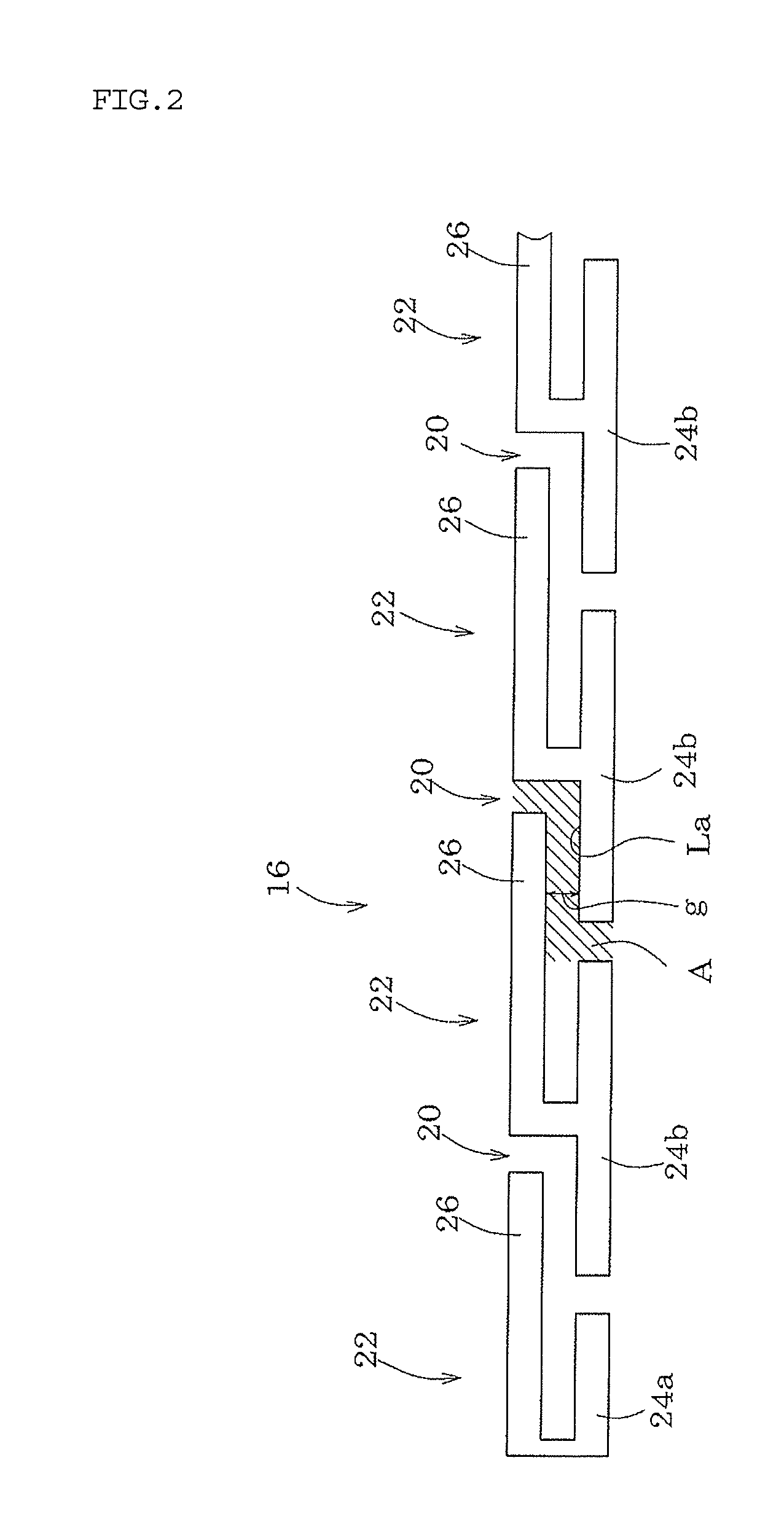
[0017]An embodiment of a touch panel according to the present invention is described. The touch panel is of a resistive type, and particularly of a 5-wire type. In a 5-wire touch panel, two substrates oppose each other at a particular distance, and rectangular resistive films are formed on the opposing surfaces of the substrates, respectively. Spacers are provided between the substrates so that when one of the substrates bends by being pressed by a finger or the like, the resistive films of both substrates make contact with each other. As the substrates, a plastic substrate formed of polyester or the like, or a glass substrate formed of soda glass or the like is used. As the resistive films, ITO (Indium Tin Oxide) or the like is used. The substrates and the resistive films are both transparent. Electrodes are formed on the four sides of either one of the resistive films. The present invention is characterized by the electrodes. The peripheral circuitry and the like other than the electrodes may be the same as those of the related art.
[0018]As shown in FIG. 1, in a touch panel 10, a rectangular resistive film 14 is formed on a substrate 12, and electrodes 16 are linearly arranged along the four sides of the resistive film 14. The electrodes 16 are placed as close to the periphery of the resistive film 14 as possible so that the usable area of the resistive film 14 may increase. To the electrodes 16, voltage is applied from power supply terminals 18 attached to the four corners of the resistive film 14. Each electrode 16 is divided into a plurality of electrodes (hereinafter, “divided electrodes 22”) by a plurality of gaps 20. The divided electrodes
Problems solved by technology
However, it is difficult to design the T-shaped electrodes 58 disclosed in Patent Document 1, due to variations in size of the T-shap
Method used
View moreImage
Smart ImageViewing Examples
Examples
Example
[0056]10, 50, 50b: touch panel
[0057]12: substrate
[0058]14: resistive film
[0059]16: electrode
[0060]18: power supply terminal
[0061]20: gap
[0062]22: divided electrode
[0063]24a, 24b: inner electrode
[0064]26: outer electrode
[0065]28: portion across which inner electrodes oppose each other
[0066]30: insulating region
Login to view more PUM
Abstract
In a touch panel, a rectangular resistive film is formed on a substrate and electrodes are provided along the four sides of the resistive film. Each electrode includes a plurality of gaps and a plurality of divided electrodes. The divided electrodes are linearly arranged along the corresponding side of the resistive film, and the electrode, in which the divided electrodes at both ends are connected to terminals, respectively, is formed by arranging the divided electrodes of the same shape and repeating this same shape.
Description
BACKGROUND OF THE INVENTION[0001]1. Field of the Invention[0002]The present invention relates to a touch panel of an input device used in a computer and the like, and particularly relates to a 5-wire touch panel.[0003]2. Description of the Related Art[0004]Prevalent touch panels include resistive types, surface acoustic wave types, capacitive types, infrared types, and the like. Further, resistive types include those termed a 4-wire type and a 5-wire type. For example, a 5-wire touch panel is disclosed in Patent Document 1.[0005]In a 5-wire touch panel shown in FIG. 16, transparent rectangular resistive films 14 are laminated on opposing surfaces of two substrates 12a and 12b, respectively. Although not shown in the figures, spacers are provided so that both substrates 12a and 12b oppose each other at a particular distance. Electrodes 56a, 56b, 56c, and 56d are formed on the four sides of either one of the resistive films 14 (FIG. 17). The substrate on which the electrodes 56a, 56b,...
Claims
Login to view more Application Information
Patent Timeline
IPC IPC(8): G06F3/041
CPCG06F2203/04113G06F3/045
Inventor ITAYA, HISAOYAMADA, TSUTOMUHOSOE, MASAHIRO
Owner GUNZE LTD
- R&D Engineer
- R&D Manager
- IP Professional
Why Eureka
- Industry Leading Data Capabilities
- Powerful AI technology
- Patent DNA Extraction
Try Eureka
Browse by: Latest US Patents, China's latest patents, Technical Efficacy Thesaurus, Application Domain, Technology Topic.
© 2024 PatSnap. All rights reserved.Legal|Privacy policy|Modern Slavery Act Transparency Statement|Sitemap