Tft-lcd array substrate and driving method thereof

Active Publication Date: 2010-06-24
BEIJING BOE OPTOELECTRONCIS TECH CO LTD +1
View PDF8 Cites 34 Cited by
  • Summary
  • Abstract
  • Description
  • Claims
  • Application Information

AI Technical Summary

Benefits of technology

[0023]In the TFT-LCD array substrate of an embodiment of the present invention, every two pixel electrodes commonly use one gate line, which reduces the number of the gate lines and the number of scan driving chips or pins of the scan driving chips, and thus facilitates reducing production cost of the TFT-LCD. Spaces saved due to the reducing of the gate lines can be used to increase width of the gate line without affecting aperture opening ratio, so as to reduce signal delay; on the other hand, the spaces saved due to the reducing of the gate lines can also be used to improve the aperture opening ratio. Further, the present invention can also generate the column data signal through the selection switc

Problems solved by technology

Since the number of data lines is increased and the length of data lines is too long, display problems such as signal delay will be caused; if width of data lines is increased fo

Method used


Image

  • Tft-lcd array substrate and driving method thereof
  • Tft-lcd array substrate and driving method thereof
  • Tft-lcd array substrate and driving method thereof

Examples


Example

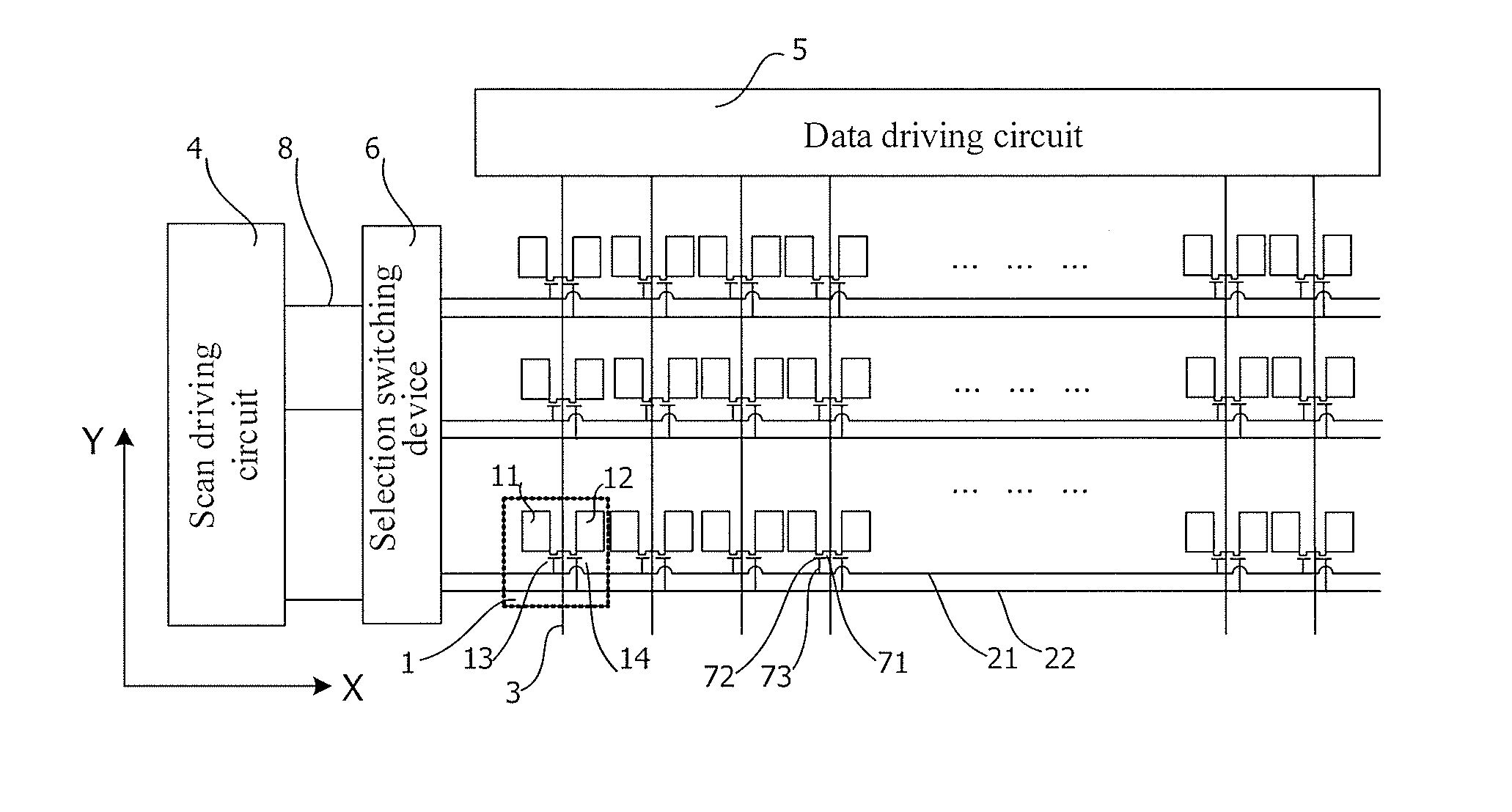
[0030]FIG. 1 is a structural schematic diagram of a first embodiment of a TFT-LCD array substrate of the present invention. As shown in FIG. 1, the TFT-LCD array substrate of the present invention comprises a substrate, on which a display region and a peripheral region outside the display region are formed; the display region consists of pixel regions arranged in matrix. Two pixel electrodes and two thin film transistors are formed in each pixel region; a selection switching device 6 is set in the peripheral region along a direction that gate lines extend (i.e., X direction as shown in FIG. 1), and the gate lines are connected to a scan driving circuit 4 through the selection switching device 6; a data driving circuit 5 is connected to the peripheral region along a direction that data lines 3 extend (i.e., Y direction as shown in FIG. 1), and data lines 3 are respectively connected to the data driving circuit 5.

[0031]The two pixel electrodes formed in each pixel region 1 are a first...

Example

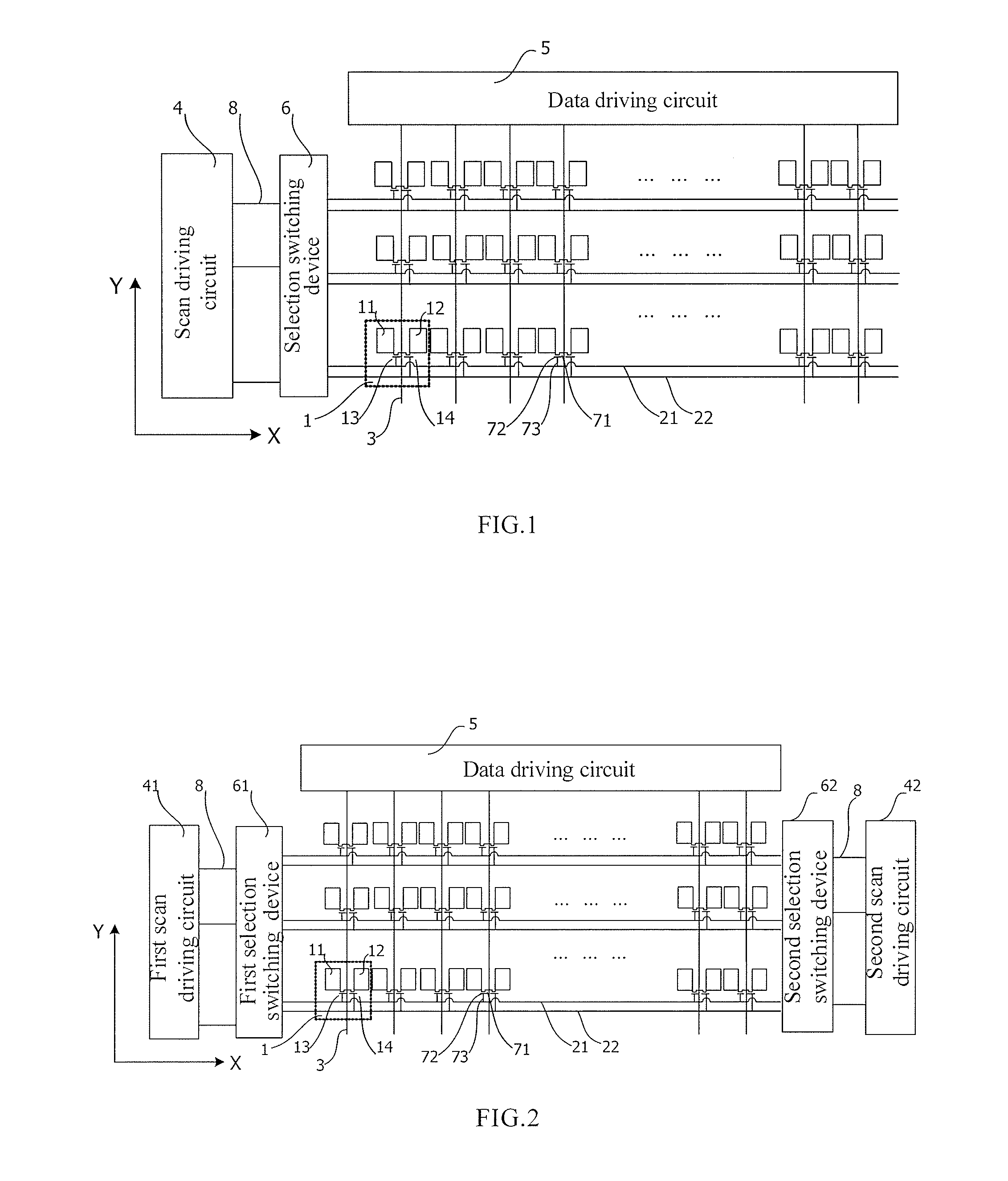
[0046]FIG. 2 is a structural schematic diagram of a second embodiment of a TFT-LCD array substrate of the present invention. The difference between the present embodiment and the embodiment illustrated in FIG. 1 lies in that in the present embodiment, peripheral regions on the left side and the right side of the display region each has one selection switching device and one scan driving circuit, and each scan driving circuit is connected to gate lines of the display region through a selection switching device. As shown in FIG. 2, a first scan driving circuit 41 is set in the peripheral region on the left side of the display region, the first scan driving circuit 41 is connected to a first selection switching device 61, and the first selection switching device 61 is connected to one end of a first gate line 21 and one end of a second gate line 22 for generating a row scan signal for a pixel row from the one end of the first gate line 21 and the one end of the second gate line 22 acco...


PUM


Abstract

The present invention relates to a TFT-LCD array substrate and a driving method thereof. The TFT-LCD array substrate comprises a substrate, on which pixel regions arranged in matrix are formed, a first pixel electrode and a first thin film transistor located in an odd column and a second pixel electrode and a second thin film transistor located in an even column are formed in each pixel region; a first gate line and a second gate line are formed in each pixel region, the first gate line is connected to gate of the first thin film transistor, and the second gate line is connected to gate of the second thin film transistor; one data line is formed in each pixel region, and the data line is connected to source of the first thin film transistor and source of the second thin film transistor, respectively. The present invention reduces the number of data lines and the number of data driving chips or the pins thereof, or, reduces the number of the gate lines and the number of scan driving chips or the pins thereof, and reduces the production cost of the TFT-LCD.

Description

TECHNICAL FIELD[0001]The present invention relates to a liquid crystal display apparatus and a driving method thereof, and in particular relates to a TFT-LCD array substrate and a driving method thereof.BACKGROUND[0002]Thin Film Transistor Liquid Crystal Display (TFT-LCD) mainly comprises a liquid crystal display panel, a scan driving circuit and a data driving circuit, wherein the liquid crystal display panel comprises a color film substrate and an array substrate set for a cell, and a liquid crystal layer set between these two substrates, and the scan driving circuit and the data driving circuit connect to TFT switching elements on the array substrate, respectively.[0003]In traditional TFT-LCD array substrates, one TFT switching element is controlled by one data line and one gate line, and a pixel electrode connected to the TFT switching element is driven by switching on or switching off the TFT switching element. While the array substrate operates, the data line transmits a video...

Claims


Application Information

Patent Timeline
IPC IPC(8): G02F1/1368G09G3/36
CPCG02F1/136286G09G2310/02G09G2300/0426G09G3/3648
Inventor MA, ZHANJIE
Owner BEIJING BOE OPTOELECTRONCIS TECH CO LTD
Why Eureka
Try Eureka