Semiconductor storage device and storage controlling method

a technology of semiconductor storage device and storage control method, which is applied in the direction of digital storage, memory adressing/allocation/relocation, instruments, etc., can solve the problems of previously stored information being lost and consuming a large amount of resources,

Inactive Publication Date: 2010-06-24
KK TOSHIBA
View PDF15 Cites 64 Cited by
  • Summary
  • Abstract
  • Description
  • Claims
  • Application Information

AI Technical Summary

Benefits of technology

[0011]According to another aspect of the present invention, a semiconductor storage device includes a first storage unit that has a plurality of first blocks that are data write regions; an instructing unit that issues a write instruction of writing data into the first blocks; a converting unit that converts an external address of input data to a memory position in the first block with reference to a conversion table in which external addresses of the data are associated with memory positions of the data in the blocks; a managing unit that manages a memory status of the data in the first blocks; and a judging unit that judges whether the first blocks includes any first block in which data writing would not cause loss of the valid data based on the memory positions of the input data and the memory status of the data, the valid data being the data associated with the external address, wherein the instructing unit issues the write instruction of writing the data into the first block in which the data writing would not cause loss of the valid data, when the first blocks include the first block in which the data writing would not cause loss of the valid data.
[0012]According to still another aspect of the present invention, a storage controlling method implemented in a semiconductor storage device, the method includes a second storage unit that has a plurality of second blocks that are data write regions; and a moving unit that moves the valid data stored in the first blocks to the second blocks when the first blocks does not include any first block in which the data writing would not cause loss of the valid data, wherein the instructing unit issues the write instruction of writing the data to the first blocks from which the valid data has been moved.

Problems solved by technology

A NAND flash ROM of a multiple-level-cell (MLC) type, which stores therein multiple bits in accordance with different voltages, has a mode of writing information into a memory cell one bit at a time by performing the writing several times. There is a problem in this write mode that previously stored information may be lost if power supply is cut off when information is being added into a memory cell having information therein.
For example, when an MLC NAND flash ROM in which two bits can be written in every memory cell is adopted in this system, data that is 2+1=3 times the amount of to-be-written data needs to be erased, which is a highly unnecessary amount.

Method used


Image

  • Semiconductor storage device and storage controlling method
  • Semiconductor storage device and storage controlling method
  • Semiconductor storage device and storage controlling method

Examples


first embodiment

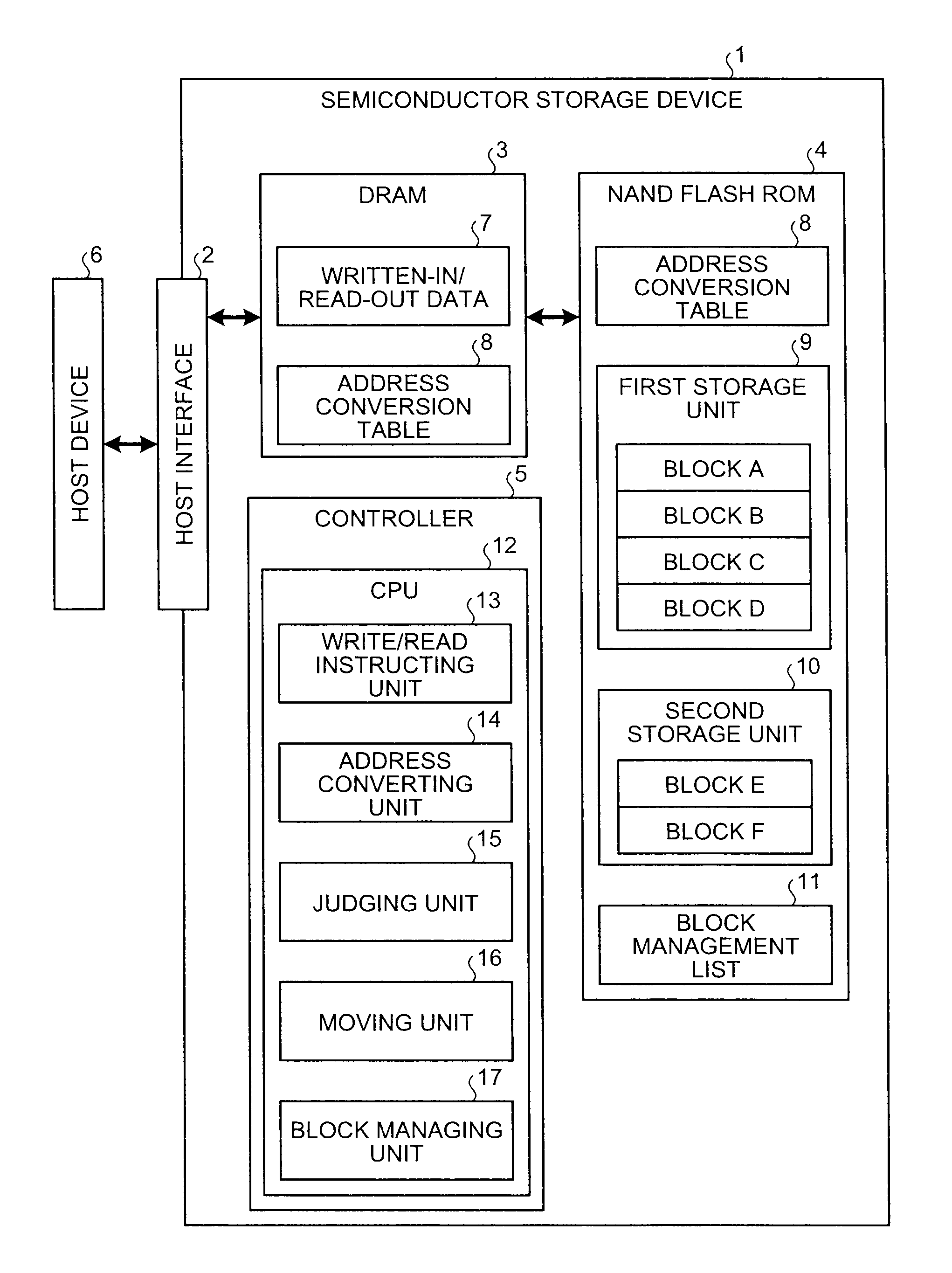
[0027]As illustrated in FIG. 1, a semiconductor storage device 1 according to the first embodiment stores data therein, and includes a host interface 2, a dynamic random access memory (DRAM) 3, a NAND flash read only memory (ROM) 4, and a controller 5. The host interface 2 performs data communications with a host device 6, such as a personal computer, to transmit and receive data.

[0028]The DRAM 3 is a memory that temporarily stores therein written data that is supplied by the host device 6, and written-in / read-out data 7 that is read from the NAND flash ROM 4 during operation. The DRAM 3 also temporarily stores therein an address conversion table 8 that is read from the NAND flash ROM 4 during operation. The address conversion table 8 will be discussed in detail later when the NAND flash ROM 4 is explained.

[0029]The NAND flash ROM 4 is of an MLC type and stores therein the data that is supplied by the host device 6 and temporarily stored in the DRAM 3. The NAND flash ROM 4 includes ...

second embodiment

[0077]According to the first embodiment, when the first storage unit has no block that does not store any valid data therein, the valid data of the blocks of the first storage unit is moved to a block of the second storage unit. In contrast, according to a second embodiment, when the first storage unit has no block that does not store therein any valid data that could become lost, the valid data stored in the blocks of the first storage unit is moved to a block of the second storage. The structure of the semiconductor storage device according to the present embodiment is explained, focusing on differences between the first and second embodiments. The rest of the structure is the same as the first embodiment, and thus the same numerals are given to such portions. The explanation thereof should be referred to the above description and is omitted here.

[0078]As explained above with reference to FIG. 2 for the first embodiment, when data is written into an upper page, a problem could ari...


PUM


Abstract

A semiconductor storage device includes a first storage unit having a plurality of first blocks as data write regions; an instructing unit that issues a write instruction of writing data into the first blocks; a converting unit that converts an external address of input data to a memory position in the first block with reference to a conversion table in which external addresses of the data are associated with the memory positions of the data in the first blocks; and a judging unit that judges whether any of the first blocks store valid data associated with the external address based on the memory positions of the input data, wherein the instructing unit issues the write instruction of writing the data into the first block in which the valid data is not stored, when any of the first blocks does not store the valid data.

Description

CROSS-REFERENCE TO RELATED APPLICATIONS[0001]This application is based upon and claims the benefit of priority from the prior Japanese Patent Application No. 2008-325632, filed on Dec. 22, 2008; the entire contents of which are incorporated herein by reference.BACKGROUND OF THE INVENTION[0002]1. Field of the Invention[0003]The present invention relates to storage control of a semiconductor storage device.[0004]2. Description of the Related Art[0005]In a semiconductor storage device incorporating a NAND flash ROM or the like, previously stored data needs to be securely protected so that it would not be corrupted when power supply is suddenly cut off during a data write operation and results in write failure. A NAND flash ROM of a multiple-level-cell (MLC) type, which stores therein multiple bits in accordance with different voltages, has a mode of writing information into a memory cell one bit at a time by performing the writing several times. There is a problem in this write mode th...

Claims


Application Information

Patent Timeline
Patent Type & Authority Applications(United States)
IPC IPC(8): G06F12/00G06F12/02
CPCG11C11/5628G11C2216/14G11C16/105G11C16/10G06F9/06G06F12/06
Inventor KANNO, SHINICHIASANO, SHIGEHIROKITSUNAI, KAZUYAYANO, HIROKUNIHIDA, TOSHIKATSU
Owner KK TOSHIBA
Why Eureka
Try Eureka