Power Management of a Spare DRAM on a Buffered DIMM by Issuing a Power On/Off Command to the DRAM Device

a technology of buffered dimms and spare drams, which is applied in the direction of memory adressing/allocation/relocation, instruments, digital storage, etc., can solve the problem that the system has not sufficiently considered the power consumption of handling redundant spare memory

Inactive Publication Date: 2010-06-24
IBM CORP
View PDF19 Cites 72 Cited by
  • Summary
  • Abstract
  • Description
  • Claims
  • Application Information

AI Technical Summary

Benefits of technology

[0009]As a result of the summarized invention, technically we have achieved a memory device with a self-timed refresh state that can be entered by a command issued across the memory device data interface to control the application of power in the system. The memory device is controlled with a power-off state where an individual device can be placed into a power-off state. A system can now have parts of the system selected to have a low power state that can be activated using a common memory interface.

Problems solved by technology

These systems have not sufficiently considered the power consumption of handling redundant spare memory.

Method used


Image

  • Power Management of a Spare DRAM on a Buffered DIMM by Issuing a Power On/Off Command to the DRAM Device
  • Power Management of a Spare DRAM on a Buffered DIMM by Issuing a Power On/Off Command to the DRAM Device
  • Power Management of a Spare DRAM on a Buffered DIMM by Issuing a Power On/Off Command to the DRAM Device

Examples


Embodiment Construction

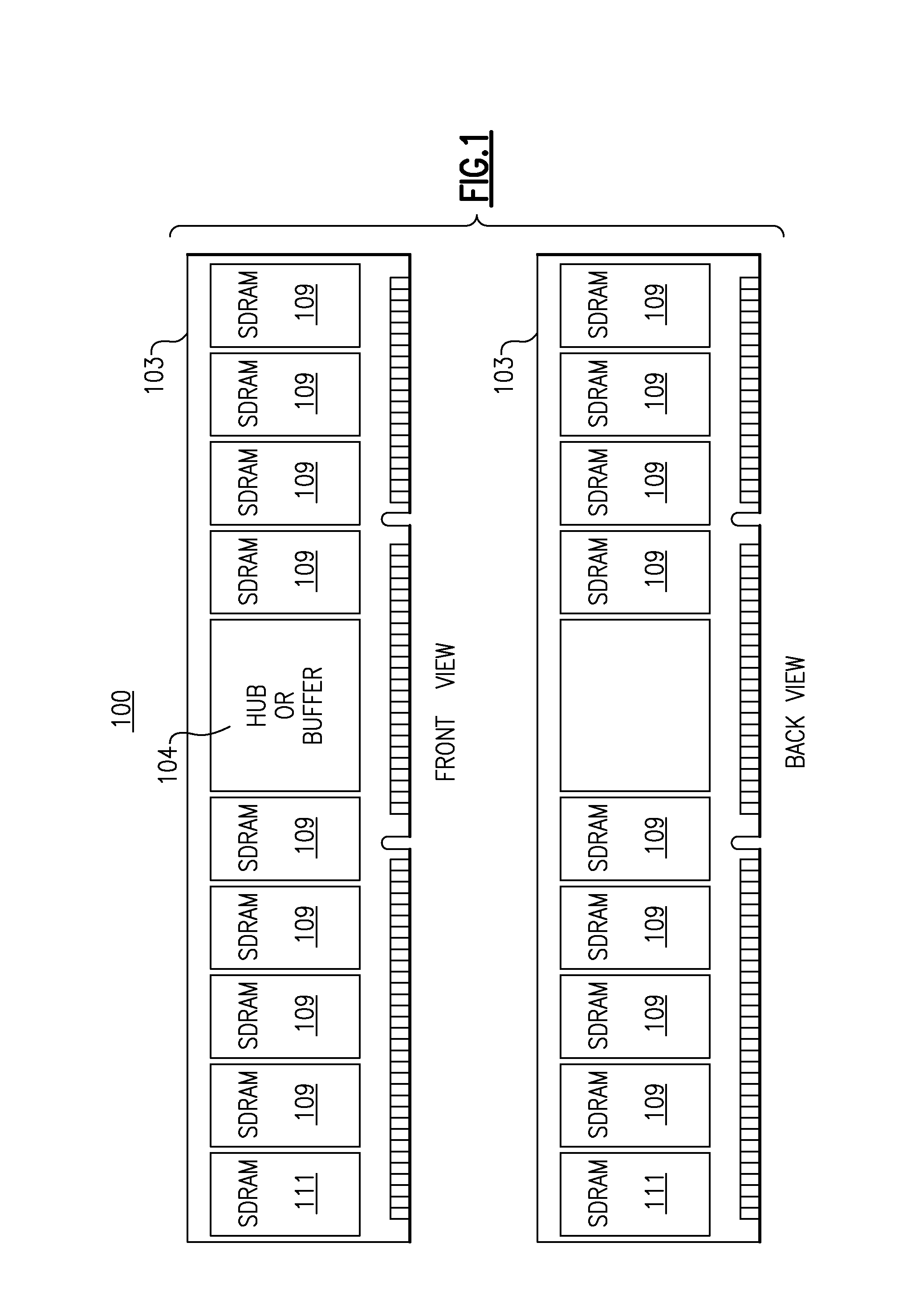
[0022]Turning now to the drawings in greater detail, it will be seen that in FIG. 1 illustrates the front and rear views of a memory sub-system in the form of a memory DIMM, which includes a hub or buffer device interfacing with multiple memory devices, including spare memory devices. FIG. 1 (100), is an example of a Dual Inline Memory Module (heretofore described as a “DIMM”) 103 shown which includes a local memory interface hub or buffer device (herein described as a “buffer” or “hub”) 104, memory devices 109 and spare memory devices 111. The front and rear of the DIMM 103 is shown, with a single buffer device 104 shown on the front of the module. In alternate exemplary embodiments, two or more buffer devices 104 may be included on module 103 in addition to more or less memory devices 109 and 111—as determined by such system application requirements as the data width of the memory interface (as provided for by memory devices 109), the DIMM density (e.g. the number of memory “ranks...


PUM


Abstract

A computer memory, having one or more of a semiconductor memory device having an internal memory array comprising a plurality of semiconductor dynamic random access memory (DRAM) cells arranged in a matrix of rows and columns, and provided as a memory module rank of such memory devices arranged in an array on a DIMM of one or more of said semiconductor memory device on a substrate which can be coupled via a memory device data interface to a memory system as a memory subsystem, each of said memory device having a low power shut-down state that can be activated using a common memory data interface. Control of power to a DRAM issues over the data interface two commands to a DRAM power control command decode, a power-state program signal and a power-state reset signal as a power-state control commands to control the power state of said DRAM, and to activate for READ/WRITE a memory cell as a normal active or spare device.

Description

TRADEMARKS[0001]IBM® is a registered trademark of International Business Machines Corporation, Armonk, N.Y., U.S.A. Other names used herein may be registered trademarks, trademarks or product names of International Business Machines Corporation or other companies.BACKGROUND OF THE INVENTION[0002]1. Field of the Invention[0003]This invention relates to computer memory, and particularly to power management for DRAMs which allow issuing a power on / off command to a DRAM device on a DIMM.[0004]2. Description of Background[0005]Before our invention synchronous dynamic random access memory (SDRAMs or DRAMs) were employed on on DIMMs or memory modules in computer systems and a standing spare memory cell or device was used to replace a failed memory cell or device. As an example, repairable fully-buffered memory modules have been used in personal computers which have spare or redundant repair memory that is accessed for repair addresses on the memory module. A repair controller has been used...

Claims


Application Information

Patent Timeline
Patent Type & Authority Applications(United States)
IPC IPC(8): G06F1/32G06F12/06
CPCG11C5/04G11C11/4074G11C5/14G11C5/06
Inventor MAULE, WARREN EDWARDGOWER, KEVIN C.KIM, KYU-HYOUNVANSTEE, DUSTIN JAMES
Owner IBM CORP
Why Eureka
Try Eureka