Dielectric Punch-Through Stoppers for Forming FinFETs Having Dual Fin Heights

a technology of dielectric punch-through stoppers and fins, which is applied in the direction of semiconductor devices, electrical apparatus, transistors, etc., can solve the problems of high manufacturing cost, low efficiency, and low efficiency of fin-height variation, so as to improve carrier mobility, improve formation accuracy, and reduce the current of punch-through fins

Active Publication Date: 2010-07-01
TAIWAN SEMICON MFG CO LTD
View PDF79 Cites 215 Cited by
  • Summary
  • Abstract
  • Description
  • Claims
  • Application Information

AI Technical Summary

Benefits of technology

[0014]The advantageous features of the embodiments of the present invention include improved accuracy in the formation of dual-fin-height

Problems solved by technology

However, the manufacturing cost is high.
By using this method with a high impurity concentration, although the punch-through currents are reduced, the carrier mobility is adversely reduced.
The structure as shown in FIG. 4 also suffers from the fin-height variation problem and the degraded carrier mobility due to th

Method used


Image

  • Dielectric Punch-Through Stoppers for Forming FinFETs Having Dual Fin Heights
  • Dielectric Punch-Through Stoppers for Forming FinFETs Having Dual Fin Heights
  • Dielectric Punch-Through Stoppers for Forming FinFETs Having Dual Fin Heights

Examples


Embodiment Construction

[0022]The making and using of the embodiments of the present invention are discussed in detail below. It should be appreciated, however, that the embodiments of the present invention provide many applicable inventive concepts that can be embodied in a wide variety of specific contexts. The specific embodiments discussed are merely illustrative of specific ways to make and use the invention, and do not limit the scope of the invention.

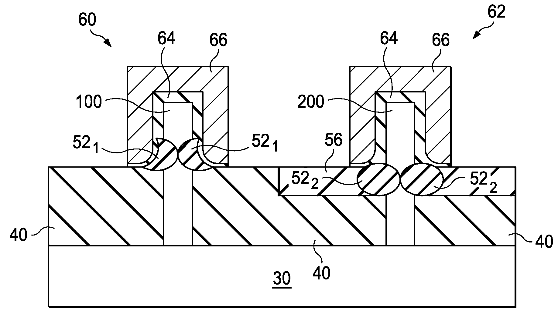
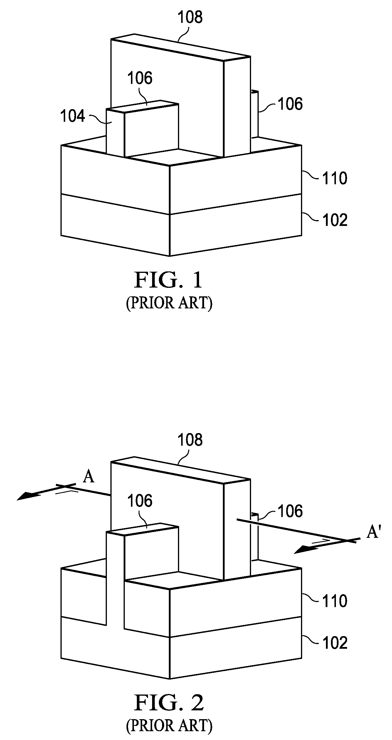
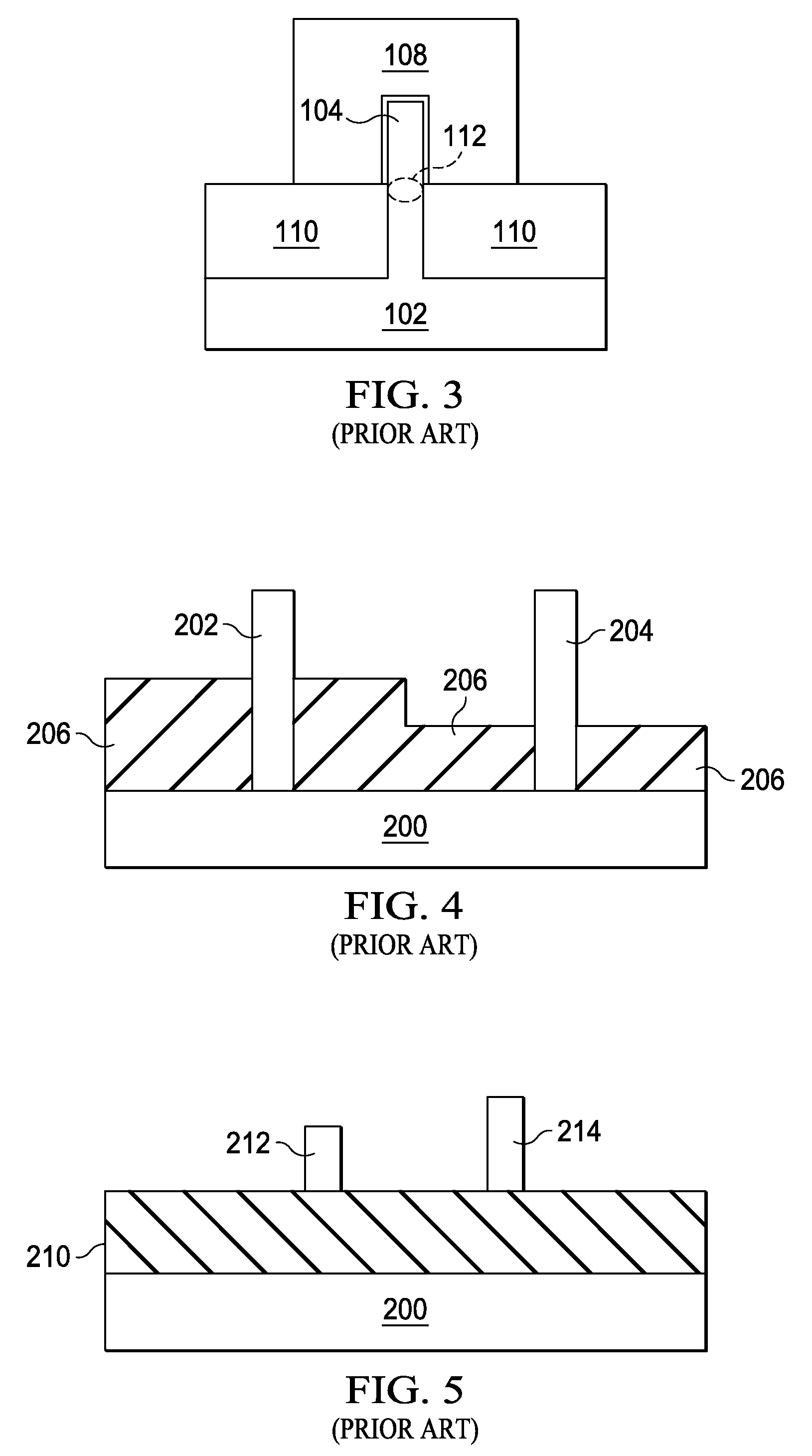
[0023]Integrated circuit formation processes including the formation of two fins with different fin heights, which fins are used for forming fin field-effect transistors (FinFETs, also referred to as multi-gate transistors or tri-gate transistors), are provided. The intermediate stages of manufacturing embodiments of the present invention are illustrated. The variations of the embodiments are discussed. Throughout the various views and illustrative embodiments of the present invention, like reference numbers are used to designate like elements.

[0024]Ref...


PUM


Abstract

A semiconductor structure includes a semiconductor substrate having a first portion and a second portion. A first Fin field-effect transistor (FinFET) is formed over the first portion of the semiconductor substrate, wherein the first FinFET includes a first fin having a first fin height. A second FinFET is formed over the second portion of the semiconductor substrate, wherein the second FinFET includes a second fin having a second fin height different from the first fin height. A top surface of the first fin is substantially level with a top surface of the second fin. A punch-through stopper is underlying and adjoining the first FinFET, wherein the punch-through stopper isolates the first fin from the first portion of the semiconductor substrate.

Description

CROSS-REFERENCE TO RELATED APPLICATION[0001]This application relates to commonly assigned U.S. patent application Ser. No. 12 / 116,074, filed May 6, 2008, entitled “FinFETs Having Dielectric Punch-Through Stoppers,” which patent application is incorporated herein by reference.TECHNICAL FIELD[0002]This invention relates generally to semiconductor devices, and particularly to structures and formation methods of Fin field-effect transistors (FinFETs).BACKGROUND[0003]With the increasing downscaling of integrated circuits and increasingly higher requirements for integrated circuits, transistors need to have higher drive currents with increasingly smaller dimensions. Fin field-effect transistors (FinFETs) were thus developed. FIGS. 1 and 2 illustrate perspective views of conventional FinFETs. Fins 104 are formed as vertical silicon fins extending above substrate 102, and are used to form source and drain regions 106 and channel regions therebetween (not shown). Vertical gates 108 intersect...

Claims


Application Information

Patent Timeline
IPC IPC(8): H01L29/772
CPCH01L29/66795H01L29/785H01L29/1083H01L21/823431H01L21/823481H01L21/76202
Inventor HUNG, SHIH-TINGCHANG, CHENG-HUNGLEE, CHEN-YIYEH, CHEN-NANYU, CHEN-HUA
Owner TAIWAN SEMICON MFG CO LTD
Why Eureka
Try Eureka