Set algorithm for phase change memory cell

a memory cell and phase change technology, applied in the field of memory devices, can solve the problems of high resistance interface within the electrical conduction path, reliability issues and bit errors of those memory cells, and achieve the effect of improving endurance, reliability and data storage performan

Active Publication Date: 2010-07-01
MACRONIX INT CO LTD
View PDF7 Cites 17 Cited by
  • Summary
  • Abstract
  • Description
  • Claims
  • Application Information

AI Technical Summary

Benefits of technology

[0012]Memory devices and methods for operating such devices described herein address the set failure mode and result in improved endurance, reliability and data storage performance. Set operations described herein comprise applyi...

Problems solved by technology

However, since the active region undergoes a phase change as a result of heating, during operation issues such as compositional changes in the phase change material within the active region can result in the formation of a high resistance interface within the electrical conduction path of ...

Method used


Image

  • Set algorithm for phase change memory cell
  • Set algorithm for phase change memory cell
  • Set algorithm for phase change memory cell

Examples


first embodiment

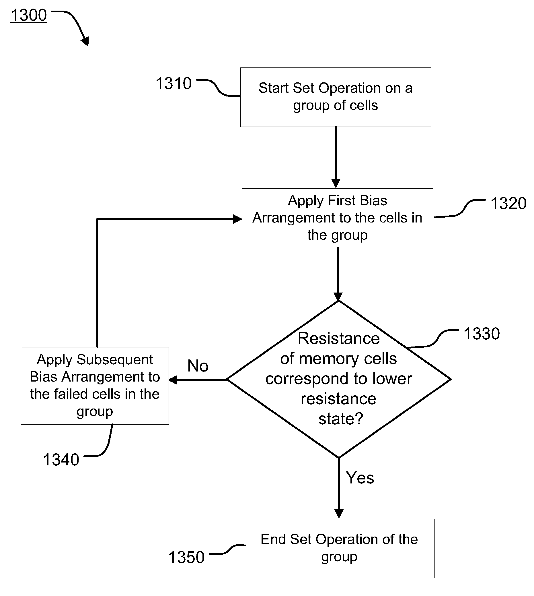
[0051]FIG. 6 is a flow diagram of a set operation 600 for programming memory cell 532 from a higher resistance state to a lower resistance state. FIG. 7 illustrates an embodiment of a timing diagram of the set operation 600 of FIG. 6. As will be understood the timing diagram of FIG. 7 is simplified and not necessarily to scale.

[0052]The set operation 600 for selected memory cell 532 begins at step 610. Step 610 may include, or in some embodiments be preceded by, a read operation to determine if the selected memory cell 532 need to be programmed by the set operation 600. The read operation can be accomplished by applying a read bias arrangement such as supplying voltages to word line 558 and bit line 560 sufficient to turn on the access transistor of the selected memory cell 532 and to induce current to flow in path 580 on the bit line 560 and through the memory element 548 to the source line 554 (which is terminated to ground in this example). The current is insufficient for the mem...

second embodiment

[0069]FIG. 10 illustrates a set operation 1000 in which the retry (or second) bias arrangement 1040 does not include the first bias arrangement of step 620, and instead includes the function of setting the memory cell 532. FIG. 11 illustrates an embodiment of a timing diagram of the set operation 1000 of FIG. 10. As will be understood the timing diagram of FIG. 11 is simplified and not necessarily to scale.

[0070]Referring to FIGS. 11 and 12, in the illustrated embodiment the retry (or second) bias arrangement of step 1040 comprises applying a voltage VWL-RETRY to word line 558, and applying a voltage pulse to the bit line 560 having a shape with initial pulse height of VHIGH and a trailing edge in which the voltage on the bit line 560 decreases with time as shown. The voltage pulse is sufficient to breakthrough the high resistance layer and induces current to flow in path 580 and provide energy to the phase change material of memory element 548.

[0071]As represented heuristically in ...


PUM


Abstract

Memory devices and methods for operating such devices are described herein. A method is described herein for operating a memory cell comprising phase change material and programmable to a plurality of resistance states including a high resistance state and a lower resistance state. The method comprises applying a first bias arrangement to the memory cell to establish the lower resistance state, the first bias arrangement comprising a first voltage pulse. The method further comprises determining whether the memory cell is in the lower resistance state, and if the memory cell is not in the lower resistance state then applying a second bias arrangement to the memory cell. The second bias arrangement comprises a second voltage pulse having a pulse height greater than that of the first voltage pulse.

Description

BACKGROUND OF THE INVENTION[0001]1. Field of the Invention[0002]The present invention relates to memory devices based on phase change based memory materials, including chalcogenide based materials and on other programmable resistive materials, and methods for operating such devices.[0003]2. Description of Related Art[0004]Phase change based memory materials, like chalcogenide based materials and similar materials, can be caused to change phase between an amorphous state and a crystalline state by application of electrical current at levels suitable for implementation in integrated circuits. The generally amorphous state is characterized by higher electrical resistivity than the generally crystalline state, which can be readily sensed to indicate data. These properties have generated interest in using programmable resistive material to form nonvolatile memory circuits, which can be read and written with random access.[0005]In phase change memory, data is stored by causing transitions...

Claims


Application Information

Patent Timeline
IPC IPC(8): G11C11/00
CPCG11C13/0004G11C13/0038G11C13/0069G11C2013/0071G11C2013/009G11C2013/0092G11C2213/79
Inventor LEE, MING-HSIU
Owner MACRONIX INT CO LTD
Why Eureka
Try Eureka