

Imaging lens, imaging device, portable terminal, and method for manufacturing imaging lens
a technology of imaging lens and portable terminal, which is applied in the direction of instruments, cameras, optical elements, etc., can solve the problems that imaging lenses cannot be easily compatible with further size reduction, and achieve the effects of convenient manufacturing of imaging lenses, and satisfactory aberration correction performan
- Summary
- Abstract
- Description
- Claims
- Application Information
AI Technical Summary
Benefits of technology
Problems solved by technology
Method used
Image

Examples
embodiment 1
[0156][▪ Imaging Device and Portable Terminal]
[0157]Typically, imaging lenses are suitably used in digital appliances (for example, portable terminals) equipped with an image capturing capability. This is because a digital appliance including a combination of an imaging lens, an image sensor, etc. functions as an imaging device that optically takes in an image of a subject and outputs it in the form of an electrical signal.
[0158]An imaging device is a main component (optical device) of a camera that shoots still and moving images of a subject, and includes, for example, from the object (i.e. subject) side thereof, an imaging lens that forms an optical image of an object and an image sensor that converts the optical image formed by the imaging lens into an electrical signal.
[0159]Examples of cameras include digital cameras, video cameras, monitoring cameras, vehicle-mounted cameras, and videophone cameras. Cameras may also be incorporated in, or externally fitted to, personal compute...
examples 1 to 4
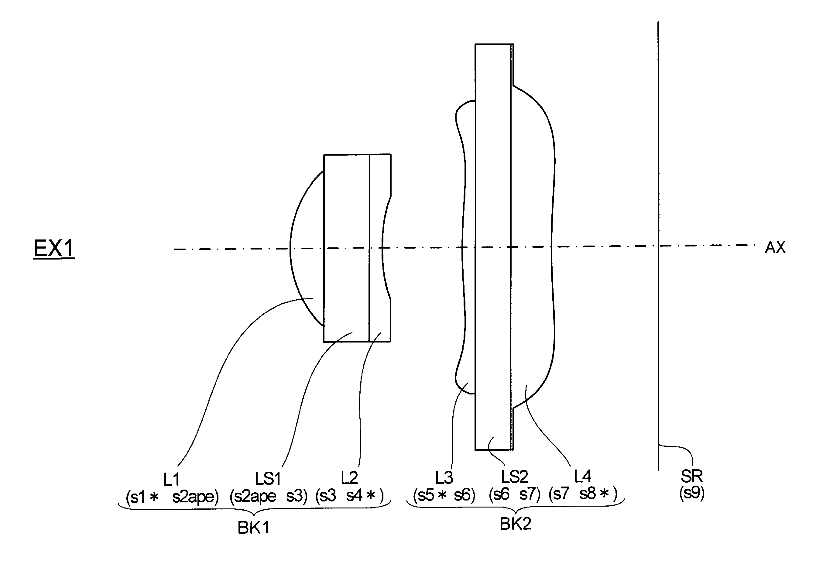
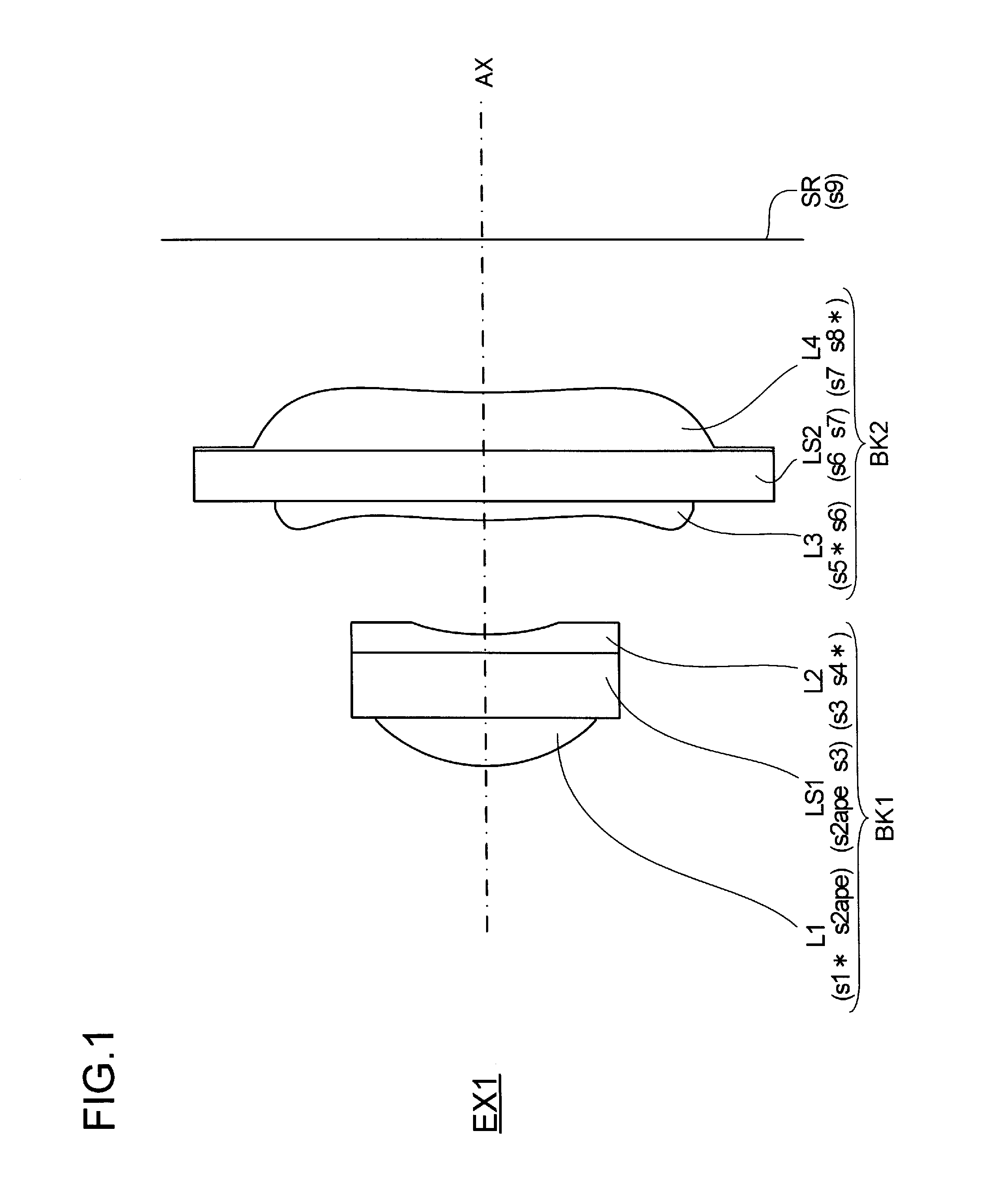
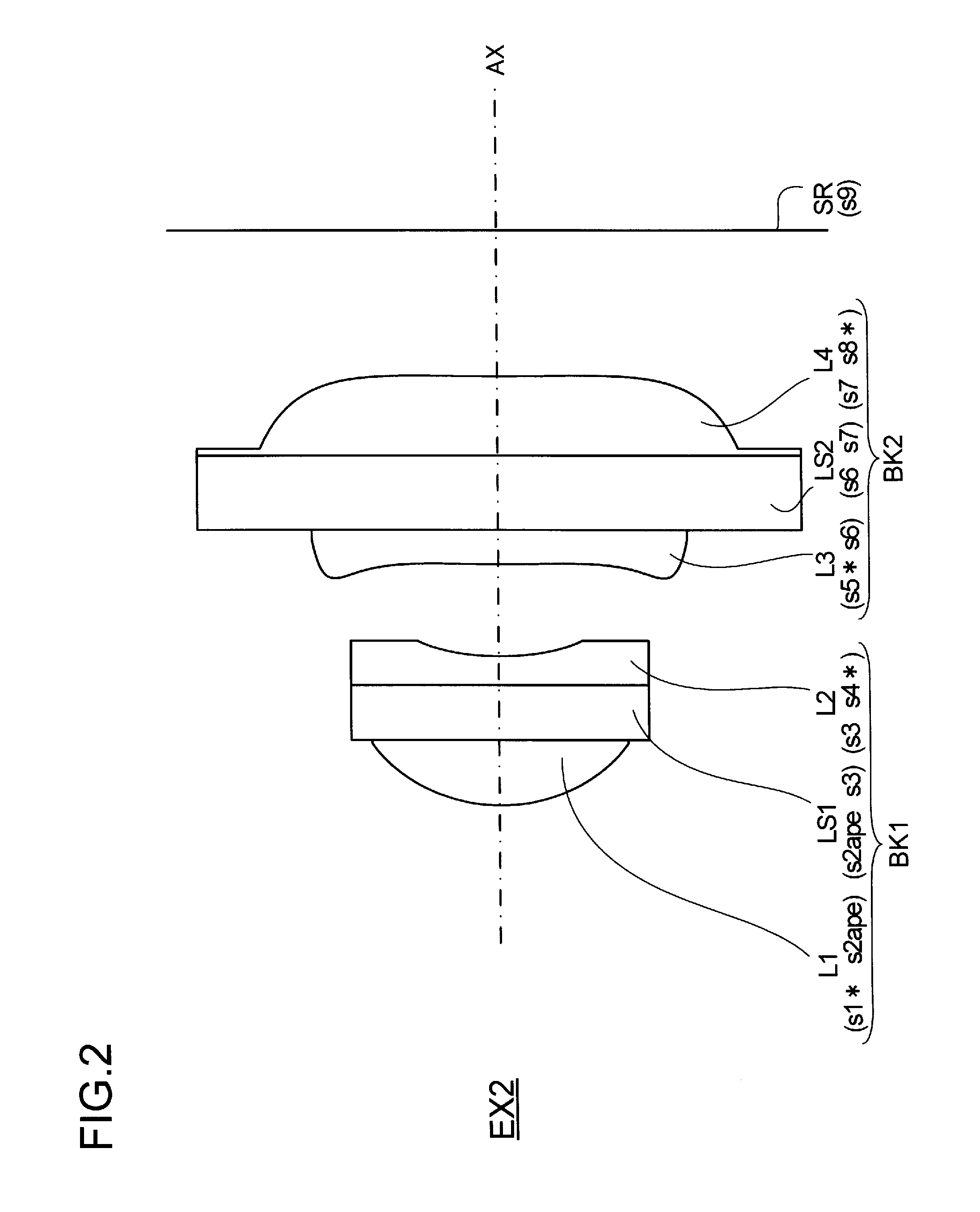
[0205]In any of Examples 1 to 4, the imaging lens LN includes two lens blocks BK1 and BK2 disposed in this order from the object side to the image side, and also includes an aperture stop ape.
[0206]The first lens block BK1 disposed at the most object-side position includes a first lens substrate LS1. A first lens L1 (lens L[LS1o]) is contiguous with the object-side substrate surface of the first lens substrate LS1, and a second lens L2 (lens L[LS1m]) is contiguous with the image-side substrate surface of the first lens substrate LS1. Specifically, the first lens L1 and the second lens L2 are configured as noted below. The aperture stop ape is formed at the boundary surface between the first lens L1 and the first lens substrate LS1.[0207]The 1st lens L1 is a plano-convex lens convex to the object side (its object-side lens surface being an aspherical surface); and[0208]The 2nd lens L2 is a plano-concave lens concave to the image side (its image-side lens surface being an aspherical s...
example 1
[0354]
TABLE 1EXAMPLE 1f [mm] 2.955Fno 2.8BF [mm] 0.9280Y′ [mm] 1.750ω [°] 30.63TL [mm] 3.177siir [mm]id [mm]iNdνdElements1*10.91110.29011.507154.00L1BK1s2ape2∞20.39021.487570.44LS1s33∞30.11031.573729.00L2s4*41.56440.684s5*53.61150.11541.507154.00L3BK2s66∞60.30451.487570.44LS2s77∞70.35561.507154.00L4s8*85.35380.928s99∞SR
TABLE 2EXAMPLE 1Aspherical Surface Datasis1s4s5s8K6.08E−035.15E+00−4.71E+014.12E−01A−4.68E−037.41E−02−7.85E−02−6.53E−02B9.08E−021.47E−01−4.45E−02−2.39E−02C−9.80E−027.91E−02−2.47E−02−8.17E−03D−5.25E−011.48E−01−3.66E−062.68E−03E−6.08E−01−1.24E+001.20E−02−1.28E−03F5.71E+00−1.42E+001.39E−02−5.39E−04
PUM
| Property | Measurement | Unit |
|---|---|---|
| particle diameter | aaaaa | aaaaa |
| optical power | aaaaa | aaaaa |
| distance | aaaaa | aaaaa |
Abstract
Description
Claims
Application Information