Chip package structure and method for fabricating the same

a technology of light-emitting chips and package structures, applied in semiconductor/solid-state device manufacturing, electrical equipment, semiconductor devices, etc., can solve the problems of insufficient chip area for conductive paths between chips and outside features formation, and the inability to reduce fabrication costs

Inactive Publication Date: 2010-07-22
XINTEC INC
View PDF4 Cites 24 Cited by
  • Summary
  • Abstract
  • Description
  • Claims
  • Application Information

AI Technical Summary

Benefits of technology

[0025]The exemplary embodiments of the chip package structure 500 have the following advantages. For example, the chip package structure is fabricated by a wafer level package process to package the chip array. Therefore, the chip package structure has much smaller dimensions than that of the conventional wire-bonding type chip package structure. When the chip package structure is arranged in a pixel array for illumination or display, an exemplary embodiment of the chip package structure may allow the pixel array to have a smaller pitch between each light emitting device. Therefore, improving pixel continuity and visual effect. Additionally, the conductive path is constructed by laminated the upper and lower holes, wherein the upper and lower holes further comprise a lateral conductive layer therebetween to increase conductive area of the hole conducting layers.

Problems solved by technology

Therefore, the chip area for conductive paths between chips and outside features formation is not enough.
The fabrication cost can not be reduced due to a huge amount of the golden wires using as I / O connections between chip arrays and outside features, especially in package structure composed by optoelectronic chips.

Method used


Image

  • Chip package structure and method for fabricating the same
  • Chip package structure and method for fabricating the same
  • Chip package structure and method for fabricating the same

Examples


Embodiment Construction

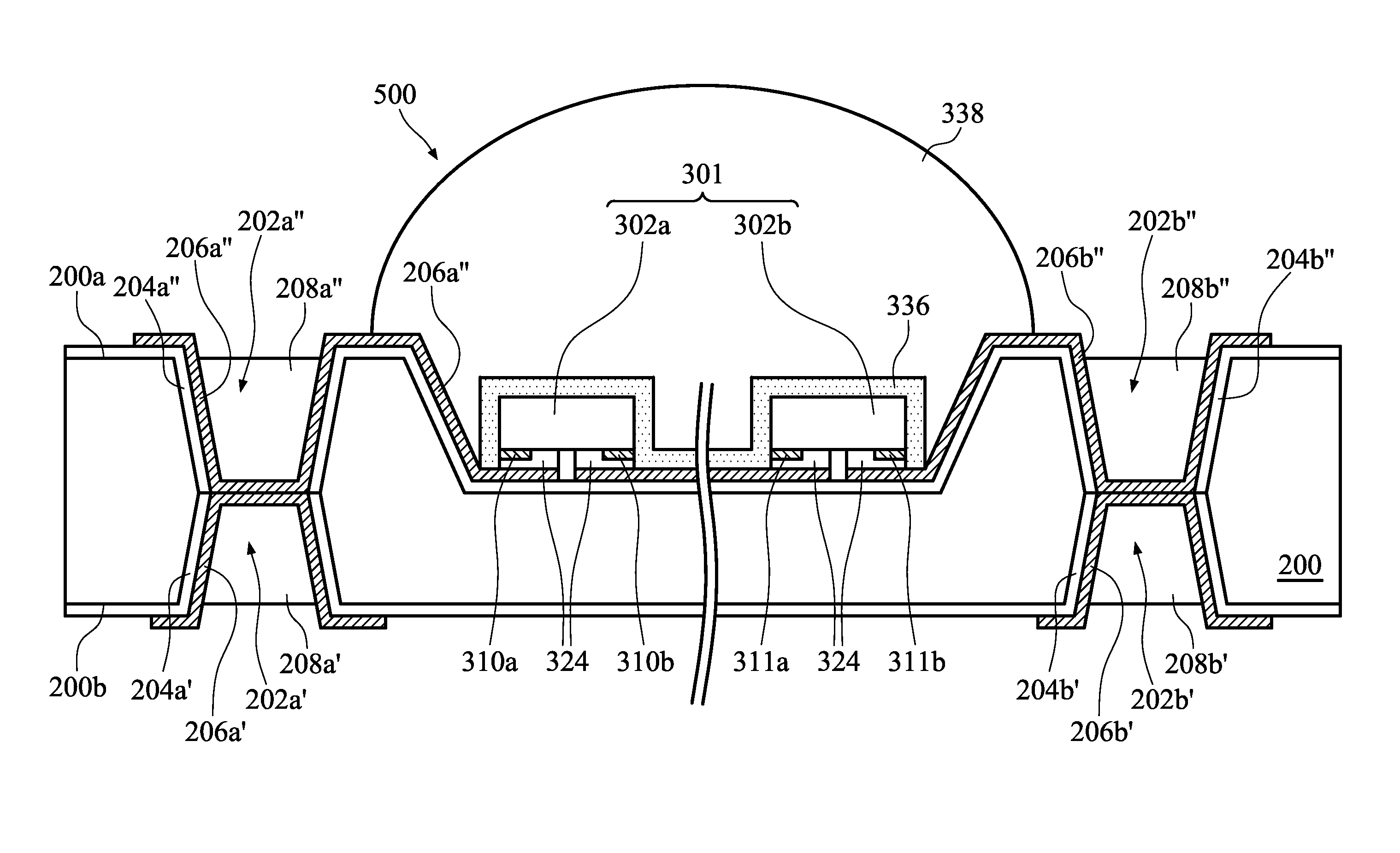
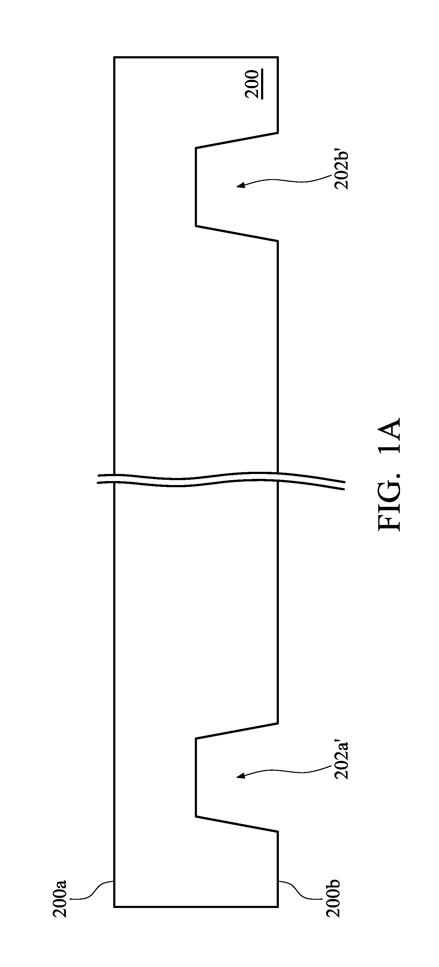
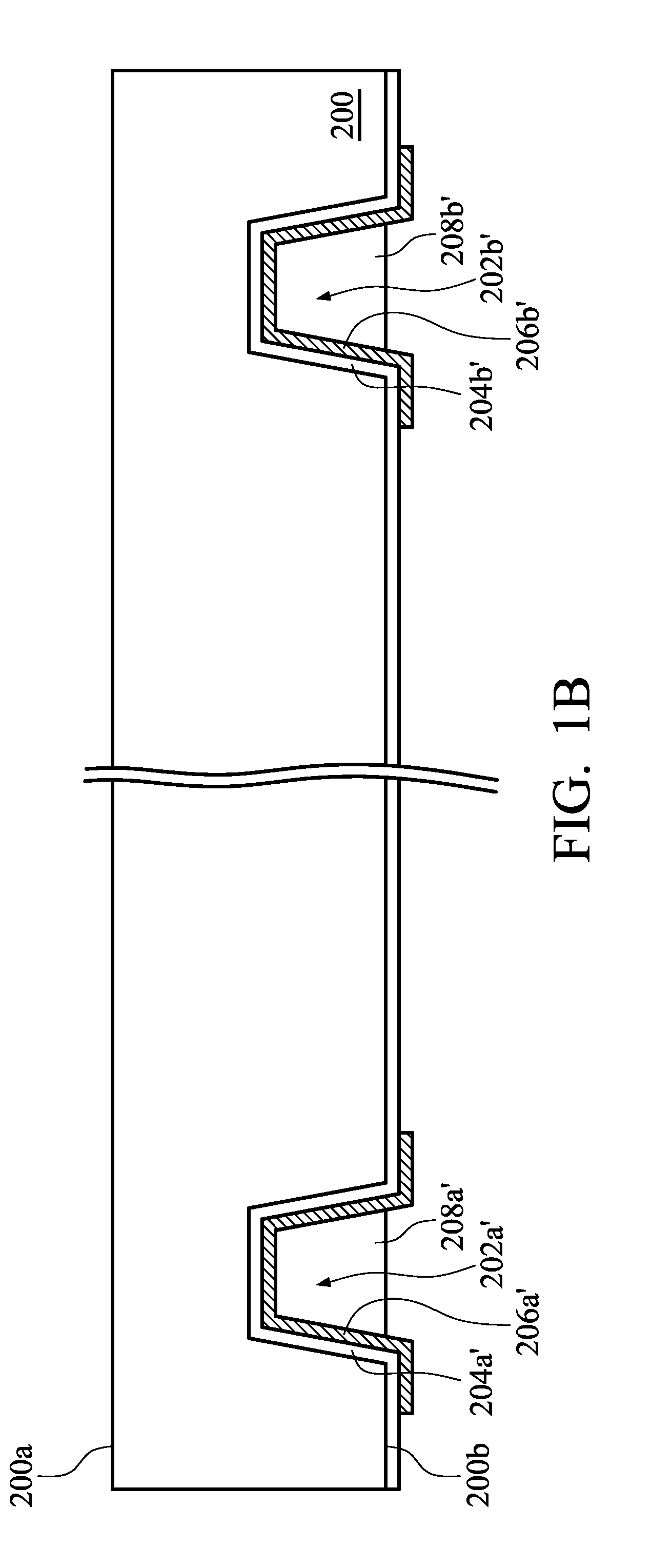
[0007]The following description is of a mode for carrying out the invention. Wherever possible, the same reference numbers are used in the drawings and the descriptions to refer the same or like parts. In the drawings, the size of some of the elements may be exaggerated and not drawn to scale for illustrative purposes. The dimensions and the relative dimensions do not correspond to actual dimensions to practice of the invention. This description is made for the purpose of illustrating the general principles of the invention and should not be taken in a limiting sense.

[0008]Embodiments of the package structure for chips of the invention packaged by a wafer level packaging (WLP) process may be applied to active or passive devices, or electronic components with digital or analog circuits, such as optoelectronic devices, micro electro mechanical systems (MEMS), micro fluidic systems, and physical sensors for detecting heat, light, or pressure. Particularly, a wafer level packaging (WLP)...


PUM


Abstract

The invention provides a chip package structure and method for fabricating the same. The chip package structure includes a carrier substrate. A plurality of isolated conductive layers is disposed on the carrier substrate. At least one chip is disposed on the carrier substrate, wherein the chip has a plurality of electrodes. The electrodes are electrically connected to the conductive layers. A conductive path is disposed in the carrier substrate, electrically connected to the electrodes through the conductive layers, wherein the conductive path comprises a plurality of laminating holes.

Description

FIELD OF THE INVENTION [0001]The present invention relates to a chip package structure and method for forming the same, and in particular relates to a light emitted chip package structure and method for forming the same.DESCRIPTION OF THE RELATED ART [0002]The chip packaging process is one of the important processes for forming chips. A chip package structure, not only provides an interface for connecting chips to electronic elements, but also provides protection for chips from environmental contaminants, along with other functions.[0003]With increasing development of the semiconductor fabrication process, chips are being formed in smaller and smaller dimensions. However, due to the ever-decreasing size and the ever-increasing density of the chips, number and density of the input / output (I / O) connections of chips have increased. Therefore, the chip area for conductive paths between chips and outside features formation is not enough. The fabrication cost can not be reduced due to a...

Claims


Application Information

Patent Timeline
Patent Type & Authority Applications(United States)
IPC IPC(8): H01L33/62H01L21/50
CPCH01L33/486H01L33/62H01L33/642H01L33/647H01L2224/73265H01L2224/92247H01L2924/1461H01L2224/48091H01L2924/00014H01L2924/00
Inventor HUANG, TIEN-HAOWU, SHANG-YITSAI, CHIA-LUN
Owner XINTEC INC
Why Eureka
Try Eureka