Display apparatus and method of driving same

a display apparatus and active matrix technology, applied in static indicating devices, instruments, electroluminescent light sources, etc., can solve the problems of complex structure of existing pixel circuits with correcting functions, adversely affecting light emission luminance, and affecting the ability to correct time-dependent variations, so as to reduce the number of components and interconnections of pixel, reduce the effect of pixel area and greatly reduce the number of interconnections

Active Publication Date: 2010-07-29
JOLED INC
View PDF7 Cites 30 Cited by
  • Summary
  • Abstract
  • Description
  • Claims
  • Application Information

AI Technical Summary

Benefits of technology

[0013]The display apparatus according to an embodiment of the present invention has a threshold voltage correcting function, a mobility correcting function, and a bootstrapping function in each of the pixels. The threshold voltage correcting function corrects a variation of the threshold voltage of the drive transistor. The mobility correcting function corrects a variation of the mobility of the drive transistor. The bootstrapping operation of the retention capacitor at the time the light-emitting device emits light is effective to keep the light emission luminance at a constant level at all times regardless of characteristic variations of an organic EL device used as the light-emitting device. Specifically, even if the current vs. voltage characteristics of the organic EL device vary with time, since the gate-to-source voltage of the drive transistor is kept constant by the retention capacitor that is bootstrapped, the light emission luminance is maintained at a constant level.
[0014]In order to incorporate the threshold voltage correcting function, the mobility correcting function, and the bootstrapping function into each of the pixels, the power supply voltage supplied to each of the pixels is applied as switching pulses. With the power supply voltage applied as switching pulses, a switching transistor for correcting the threshold voltage and a scanning line for controlling the gate of the switching transistor are not demanded. As a result, the number of components and interconnects of the pixel is greatly reduced, making it possible to reduce the pixel area for providing higher-definition display. The mobility correcting period can be adjusted based on the phase difference between the video signal and the sampling pulse by correcting the mobility simultaneously with the sampling of the video signal potential. Furthermore, the mobility correcting period can be controlled to automatically follow the level of the video signal. Because the number of components of the pixel is small, any parasitic capacitance added to the gate of the drive transistor is small, so that the retention capacitor can be bootstrapped, reliably, thereby improving the ability to correct a time-depending variation of the organic EL device.
[0015]According to an embodiment of the present invention, a display apparatus has an active-matrix display apparatus employing light-emitting devices such as organic EL devices as pixels, each of the pixels having a threshold voltage correcting function for the drive transistor, a mobility correcting function for the drive transistor, and a function to correct a time-depending variation of the organic EL device (bootstrapping function) for allowing the display apparatus to display high-quality images. Since the mobility correcting period can be set automatically depending on the video signal potential, the mobility can be corrected regardless of the luminance and pattern of displayed images. An existing pixel circuit with such correcting functions is made of a large number of components, has a large layout area, and hence is not suitable for providing higher-definition display. According to an embodiment of the present invention, however, since the power supply voltage is applied as switching pulses, the number of components and interconnects of the pixel is greatly reduced, making it possible to reduce the pixel layout area. Consequently, the display apparatus according to an embodiment of the present invention can be provided as a high-quality, high-definition, flat display unit.

Problems solved by technology

In addition, the characteristics of the organic EL devices tend to vary with time.
Such characteristic variations of the drive transistors and characteristic variations of the organic EL devices adversely affect the light emission luminance.
However, existing pixel circuits with a correcting function are complex in structure as they demand an interconnect for supplying a correcting potential, a switching transistor, and a switching pulse.
Because each of the pixel circuits has many components, they have presented obstacles to efforts to achieve a higher-definition display.

Method used


Image

  • Display apparatus and method of driving same
  • Display apparatus and method of driving same
  • Display apparatus and method of driving same

Examples


Embodiment Construction

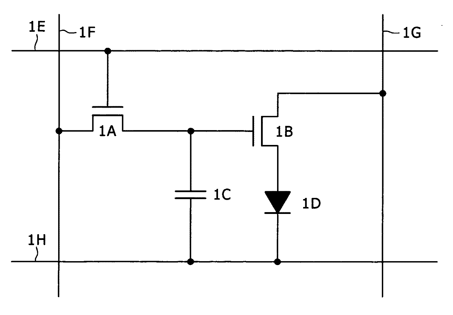
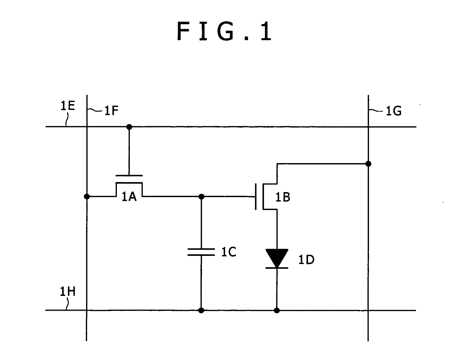
[0038]For an easier understanding of the present invention and a clarification of the background thereof, a general structure of a display apparatus will be described initially below with reference to FIG. 1. FIG. 1 is a circuit diagram showing a pixel of a general display apparatus. As shown in FIG. 1, the pixel circuit has a sampling transistor 1A disposed at the intersection of a scanning line 1E and a signal line 1F which extend perpendicularly to each other. The sampling transistor 1A is an N-type transistor having a gate connected to the scanning line 1E and a drain connected to the signal line 1F. The sampling transistor 1A has a source connected to an electrode of a retention capacitor 1C and the gate of a drive transistor 1B. The drive transistor 1B is a N-type transistor having a drain connected to a power supply line 1G and a source connected to the anode of a light-emitting device 1D. The other electrode of the retention capacitor 1C and the cathode of the light-emitting...


PUM


Abstract

A display apparatus including a pixel array and a driver configured to drive the pixel array, the pixel array having scanning lines as rows, signal lines as columns, a matrix of pixels disposed at respective intersections of the scanning lines and the signal lines, and power supply lines disposed along respective rows of the pixels, the driver having a main scanner for successively supplying control signals to the scanning lines to perform line-sequential scanning on the rows of the pixels, a power supply scanner for supplying a power supply voltage, which selectively switches between a first potential and a second potential, to the power supply lines in synchronism with the line-sequential scanning, and a signal selector for supplying a signal potential, which serves as a video signal, and a reference potential to the signal lines as the columns in synchronism with the line-sequential scanning.

Description

CROSS REFERENCES TO RELATED APPLICATIONS[0001]This is a Continuation Application of U.S. patent application Ser. No. 11 / 802,150, filed May 21, 2007, which claims priority from Japanese Patent Application JP 2006-141836 filed in the Japan Patent Office on May 22, 2006, the entire contents of which are incorporated herein by reference.BACKGROUND OF THE INVENTION[0002]1. Field of the Invention[0003]The present invention relates to an active-matrix display apparatus having light-emitting devices as pixels thereof and a method of driving such an active-matrix display apparatus.[0004]2. Description of the Related Art[0005]In recent years, growing efforts have been made to develop flat, self-emission display apparatuses using organic EL devices as light-emitting devices. An organic EL device is a device utilizing a phenomenon in which an organic thin film emits light under an electric field. The organic EL device has a low power requirement because it can be energized under a low voltage o...

Claims


Application Information

Patent Timeline
Patent Type & Authority Applications(United States)
IPC IPC(8): G09G5/00H05B44/00
CPCG09G3/3233G09G2300/0819G09G2320/043G09G2300/0866G09G2300/0842G09G3/30G09G3/32G09G3/20H05B33/12
Inventor UCHINO, KATSUHIDEIIDA, YUKIHITO
Owner JOLED INC
Why Eureka
Try Eureka