Calibration of Memory Driver With Offset in a Memory Controller and Memory Device Interface in a Communication Bus

a technology of memory controller and offset, which is applied in the direction of instruments, pulse techniques, and increasing modifications, can solve the problems of mismatch between dram and controller impedance, variable final dram training values, etc., and achieve the effect of reducing mismatches and improving timing margins

Inactive Publication Date: 2010-07-29
IBM CORP
View PDF4 Cites 36 Cited by
  • Summary
  • Abstract
  • Description
  • Claims
  • Application Information

AI Technical Summary

Benefits of technology

[0006]The present invention provides for a memory device and a memory controller, typically a DRAM memory device, and more particularly, a GDDR3 memory device, to be coupled during driver training to reduce mismatches by adjusting a voltage to the reference resistors on a DRAM device making the DRAM driver impedance vary accordingly to yield improvements in timing margins.

Problems solved by technology

However, process variations and resolution may cause variations in the final DRAM training values.
The variations may occur within a memory controller coupled to the DRAM if it trains in a similar manner, thereby causing a mismatch in DRAM and controller impedances.

Method used


Image

  • Calibration of Memory Driver With Offset in a Memory Controller and Memory Device Interface in a Communication Bus
  • Calibration of Memory Driver With Offset in a Memory Controller and Memory Device Interface in a Communication Bus
  • Calibration of Memory Driver With Offset in a Memory Controller and Memory Device Interface in a Communication Bus

Examples


Embodiment Construction

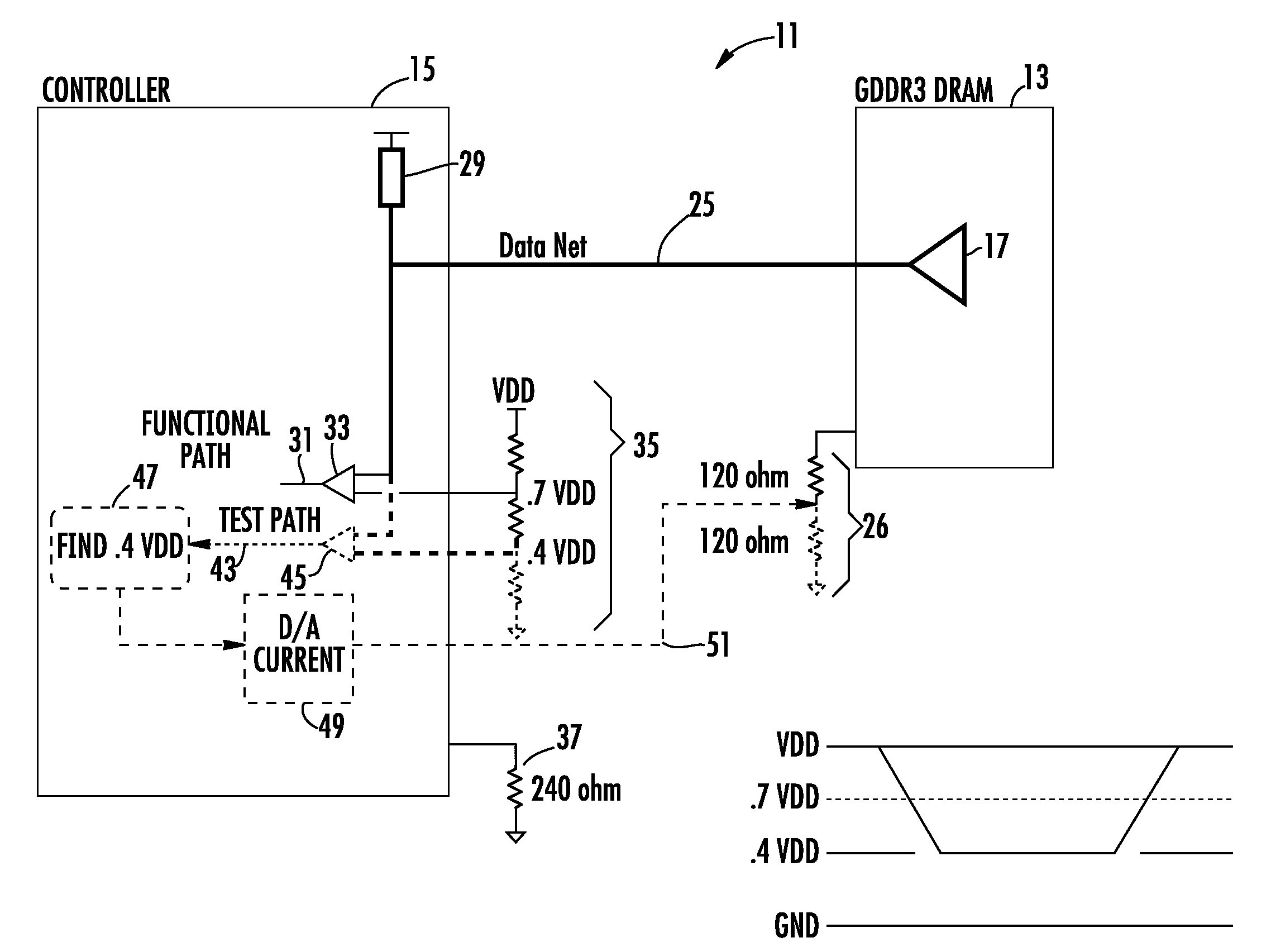
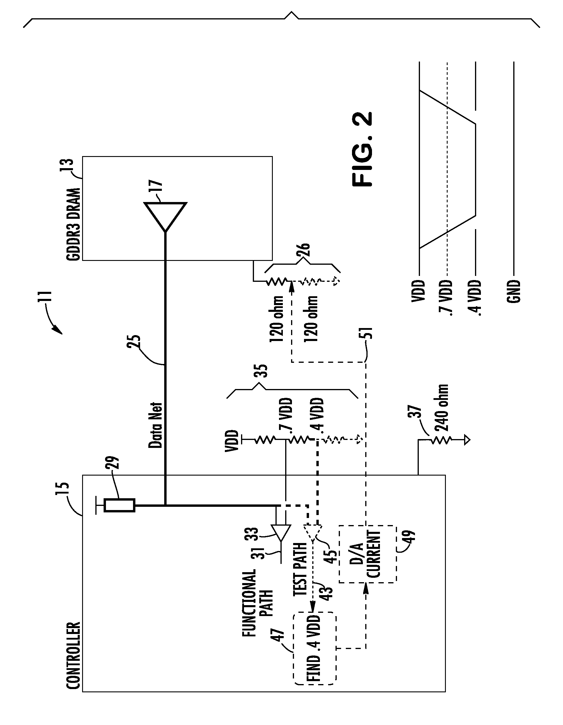
[0014]Embodiments consistent with the invention may capitalize on the ability to couple a memory device such as a DRAM and a memory controller during driver training to reduce mismatches by adjusting a voltage to the reference resistors used in driver training on the DRAM device making the driver either weaker or stronger as needed to yield improvements in timing margins. In more general terms, coupling the components on a shared electrical bus through level adjustment removes known offset issues. While embodiments of the invention are described specifically for a GDDR3 interface from a memory controller to a GDDR3 memory device, the system and method described may be applied to any number of system and sub-system electrical communication buses. Optionally, the speed at which the interface operates may be improved as a result of employing the system and method described.

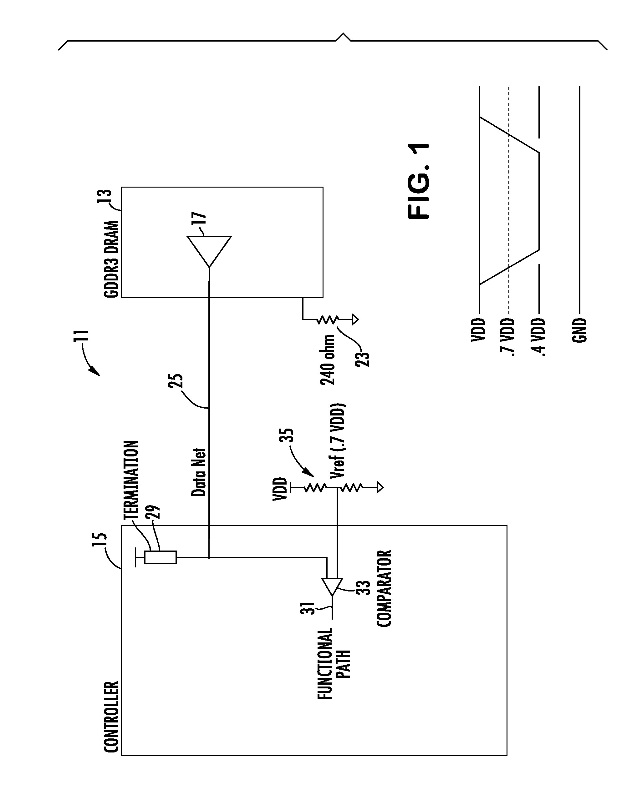
[0015]Turning more particularly to the drawings, FIG. 1 shows a typical GDDR3 interface system 11. More particular...


PUM


Abstract

A method and system are provided for coupling a DRAM and a memory controller during driver training to reduce mismatches by controlling impedances within the system environment. The memory device, which is typically the device initializing a bit level voltage on a data net, is adjusted through altering what appears to be the reference voltage value to the memory device. A current driven to the memory device is varied in small increments while impedance training is rerun until a desired value is achieved to set the 0 level voltage on the data net.

Description

RELATED APPLICATIONS[0001]The present application relates to co-pending U.S. patent applications, entitled “Setting Controller VREF in a Memory Controller and Memory Device Interface in a Communication Bus” (Docket No. ROC920080129US1), “Setting Controller Termination in a Memory Controller and Memory Device Interface in a Communication Bus” (Docket No. ROC920080130US1), “Setting Memory Controller Driver to Memory Device Termination Value in a Communication Bus” (Docket No. ROC920080132US1), “Setting Memory Device Vref in a Memory Controller and memory Device Interface in a Communication Bus” (Docket No. ROC920080133US1), and “Setting Memory Device Termination in a Memory Device and Memory Controller Interface in a Communications Bus” (Docket No. ROC920080134US1), by the present inventors, Paul W. Rudrud, Thomas W. Liang, Benjamin A. Fox, and William P. Hovis. The co-pending applications are filed concurrently herewith, and are incorporated by reference in their entireties.FIELD OF ...

Claims


Application Information

Patent Timeline
Patent Type & Authority Applications(United States)
IPC IPC(8): G11C5/14G06F13/00H03K17/16
CPCG11C5/147G11C7/1051G11C7/1057G11C11/4093H03K19/0005G11C29/022G11C29/028G11C29/50008G11C2207/2254G11C29/02
Inventor FOX, BENJAMIN AHOVIS, WILLIAM PLIANG, THOMAS WRUDRUD, PAUL
Owner IBM CORP
Why Eureka
Try Eureka