

Imprint mold
a technology of imprinting and molds, applied in the field of imprinting molds, can solve the problems of foreign particles, inability to transfer patterns to the cured portion of the transfer layer, and generation of light shielding films, so as to prevent light leakage and suppress foreign particle adhesion
- Summary
- Abstract
- Description
- Claims
- Application Information
AI Technical Summary
Benefits of technology
Problems solved by technology
Method used
Image

Examples
Embodiment Construction
[0021]Various embodiments of the present invention will be described with reference to the accompanying drawings. It is to be noted that the same or similar reference numerals are applied to the same or similar parts and elements throughout the drawings, and the description of the same or similar parts and elements will be omitted or simplified.
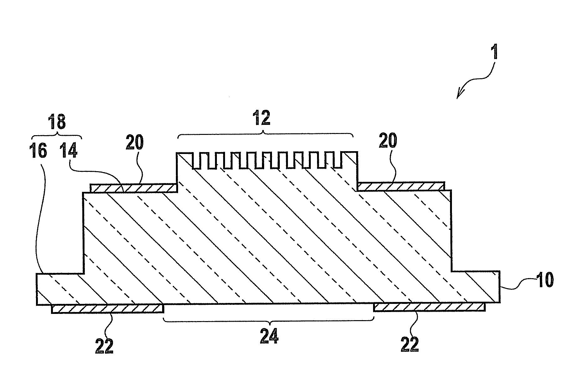
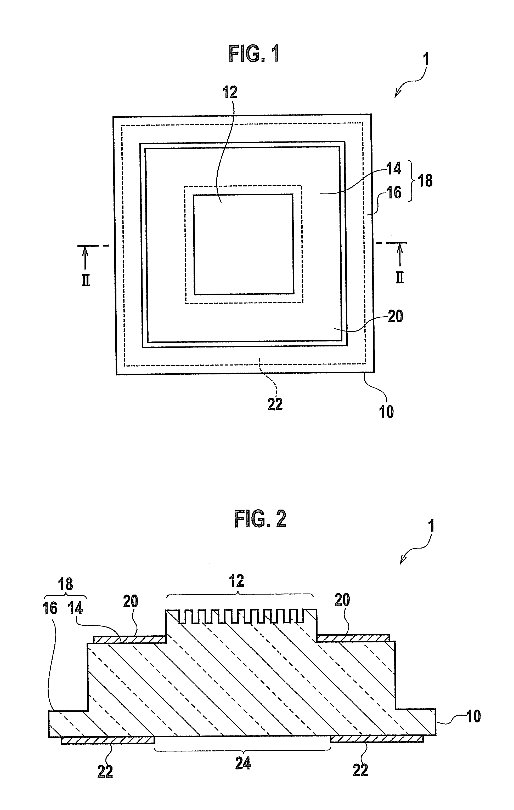
[0022]An imprint mold 1 according to an embodiment of the present invention includes a substrate 10 having a first principal surface (front surface) and a second principal surface (rear surface) opposite to the front surface, a first light shielding film 20 provided on the front surface, and a second light shielding film 22 provided on the rear surface, as shown in FIGS. 1 and 2. A pattern region 12 and an unpatterned region 18 are provided on the front surface of the substrate 10. A first region 14 provided along a periphery of the pattern region 12 and a second region 16 extending from the first region 14 to an outer edge of the substrate 1...
PUM
| Property | Measurement | Unit |
|---|---|---|
| wavelength | aaaaa | aaaaa |
| wavelength | aaaaa | aaaaa |
| thickness | aaaaa | aaaaa |
Abstract
Description
Claims
Application Information