Signal processing circuit and signal processing method

a signal processing circuit and signal processing technology, applied in the direction of digital transmission, line-transmission details, transmission monitoring, etc., can solve the problems of large rom area required to store waveform, the above-mentioned performance a little bit degrades, and the foregoing of related techniques, so as to avoid more complex configuration and high-accuracy compensating a quadrature modulator

Active Publication Date: 2010-08-05
NEC CORP
View PDF2 Cites 19 Cited by
  • Summary
  • Abstract
  • Description
  • Claims
  • Application Information

AI Technical Summary

Benefits of technology

[0067]It is therefore an object of the present invention to provide a signal processing circuit and a signal processing method which are capable of highly accurately compensating a quadrature modulator for I / Q mismatches while avoiding more complexity of configuration.

Problems solved by technology

In recent years, however, although a transmitter is required to provide higher performance in connection with increasingly faster communications, the above-mentioned performance rather tends to degrade due to constraints on circuit configuration resulting from the transition of the architecture toward direct conversion, and a reduction in voltages of the processes.
However, the foregoing related techniques imply problems described below.
The related techniques described in conjunction with FIGS. 1 through 6 have a problem in that a large ROM area is required to store waveform data of a test signal because the test signal is a smooth sinusoidal wave.
They also has a problem in that an AD converter is required to A / D convert the output of an envelope detector.
However, a problem is that an AD converter is required to A / D convert the output of the envelope detector.
Also, Patent Document 1 discloses only a method of compensating for an I / Q phase mismatch, but does not disclose a method of compensating for an I / Q amplitude mismatch.
However, a DC offset in terms of an input exists without exception in the quadrature modulator due to a problem of its manufacturing accuracy of the quadrature modulator.
Consequently, even if there is no input to the quadrature modulator, a comparable carrier leak occurs at point 0′.
In other words, the method disclosed in Patent Document 1 does not function correctly when a DC offset exists in the quadrature modulator.
Nevertheless, when a DA converter is employed, a certain amount of DC offset inevitably remains due to the problem of resolution of the DA converter.
Accordingly, to use the method disclosed in Patent Document 1, the DC offset must be removed at an accuracy significantly more strict as compared with the amount of DC offset allowed for the radio communication system, resulting in a more complicated implementation.
As a result, the method disclosed in Patent Document 1 does not correctly function.
The conventional technique disclosed in Patent Document 2 has a problem in that the configuration is more complicated, such as the need for a test signal generating part for generating a smooth sinusoidal test signal and an AD converter.
In addition to the problem in which the configuration is more complicated, the conventional technique disclosed in Patent Document 3 has a problem in that the I / Q accuracy and the like of an I / Q quadrature down converter for use in a compensation operation constitute causes for errors in the compensation operation.
However, it can be said to be contradictory that while the compensation operation is performed due to the inability to manufacture a quadrature modulator having high modulation accuracy, an I / Q quadrature down converter having a high I / Q accuracy is required as a means therefor.
The conventional techniques disclosed in Patent Documents 4, 5 also have a problem in that the configuration is more complicated, such as the need for a test signal generating part, an AD converter and the like, as mentioned above, but Patent Documents 4, 5 do not disclose means for solving this problem.
However, even with this technique, an AD converter is required.
Consequently, there is a problem in which hardware must be added in order to solve the quadruple simultaneous equations, and a problem in which the accuracy of the compensation amount exacerbates.
Also, no solution is disclosed in Patent Document 6 for a problem in which an I / Q amplitude mismatch amount must be previously found.
However, this technique also requires an AD converter.
In the conventional techniques disclosed in Patent Documents 8, 9, since a quadrature demodulator is used as a detection system in a compensation operation for I / Q phase mismatch and I / Q amplitude mismatch, a problem arises in which the accuracy of the quadrature demodulator can cause errors in the compensation operation.
However, it can be said to be contradictory that while the compensation operation is performed due to the inability to manufacture a quadrature modulator having a high modulation accuracy, a quadrature demodulator having high I / Q accuracy is required as a means therefor.
Also, if a DC offset remains in the quadrature demodulator in the compensation operation for I / Q phase mismatch, this DC offset is reflected as an offset of a compensation amount for correcting a transmission baseband signal, thus leading to an increase in carrier leakage of the quadrature modulator.
Specifically, the compensation amount for an I / Q phase mismatch must be found from data which is made available within the range of a limited resolution of the AD converter, resulting in a problem of exacerbation in the accuracy of the resulting compensation amount.

Method used


Image

  • Signal processing circuit and signal processing method
  • Signal processing circuit and signal processing method
  • Signal processing circuit and signal processing method

Examples


first exemplary embodiment

[0118]FIG. 9 is a block diagram showing the whole configuration of a signal processing circuit according to a first exemplary embodiment of the present invention.

[0119]Referring to FIG. 9, the signal processing circuit of this exemplary embodiment comprises transmission BB (baseband) signal generating part 1; test signal generating part 2; switch 3 labeled SW; I / Q mismatch compensating part 4; quadrature modulator 5; envelope detector 6; low pass filter 7; comparing part 8; and control part 9.

[0120]Transmission BB signal generating part 1 generates a transmission baseband signal in a transmission operation.

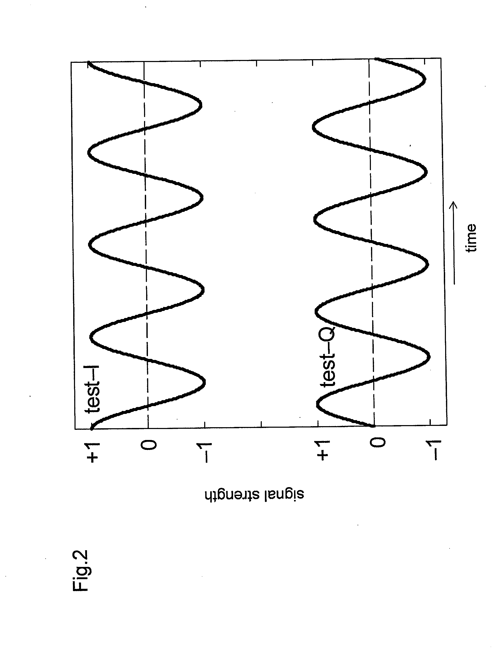
[0121]Test signal generating part 2 sequentially generates two sets of combinations of I / Q-components of test signals which are AC signals under the control of control part 9 in a compensation operation.

[0122]Switch 3 selects the test signal generated by test signal generating part 2 in a compensation operation, and selects the transmission baseband signal generated by transmissio...

second exemplary embodiment

[0221]FIG. 28 is a block diagram showing the whole configuration of a signal processing circuit according to a second exemplary embodiment of the present invention.

[0222]Referring to FIG. 28, the signal processing circuit of this exemplary embodiment differs, in comparison with the first exemplary embodiment in FIG. 10, in that I / Q mismatch compensating part 4 is preceded by DA converter 101 for transmission BB signal generating part 1, and DA converter 102 for test signal generating part 2, respectively, provided independently of each other. In other words, I / Q mismatch compensating part 4 performs I / Q mismatch compensations in an analog manner.

[0223]Switch 3 selects the output of DA converter 101 in a transmission operation, and selects the output of DA converter 102 in a compensation operation.

[0224]I / Q mismatch compensating part 4 selects the output of DA converter 101 in a transmission operation, and selects the output of DA converter 102 in a compensation operation.

[0225]In th...

third exemplary embodiment

[0228]FIG. 29 is a block diagram showing the whole configuration of a signal processing circuit according to a third exemplary embodiment of the present invention.

[0229]Referring to FIG. 29, the signal processing circuit of this exemplary embodiment differs, in comparison with the first exemplary embodiment in FIG. 10, in that a transmission baseband signal generated by transmission BB signal generating part 1 and test signals generated by test signal generating part 2 are applied to independent DA converters 101, 102 through independent I / Q mismatch compensating parts 41, 42, respectively.

[0230]This exemplary embodiment is advantageous in that requirements for a transmission operation can be compatible with those for a compensation operation when the speed and resolution required for a DA converter in the transmission operation are largely distinct from the speed and resolution required for the DA converter in the compensation operation.

[0231]In the following, a description will be...


PUM


Abstract

A signal processing circuit for compensating for an I/Q amplitude mismatch in which the amplitudes of I- and Q-components of output signals of a quadrature modulator are unequal to or for compensating for an I/Q phase mismatch in which the phase difference between the I- and the Q-components of output signals of the quadrature modulator deviates from 90 degrees. The signal processing circuit comprises an I/Q mismatch compensating part that corrects the amplitude or phase of an input signal based on the compensation amount for compensating for an I/Q amplitude mismatch or an I/Q phase mismatch and that inputs the corrected signal into a quadrature modulator; a test signal generating part that sequentially generates and inputs two sets of combined I- and Q-components of a test signal, which is an AC signal, to the I/O mismatch compensating part; a detector that determines an amplitude of the envelope of an output signal of the quadrature modulator; a filter that passes those ones of output signals of the detector which have frequencies equal to or lower than a cutoff frequency; and a control part that derives an amplitude or phase compensation amount of the I/Q mismatch compensating part such that the output values of the filter at the time of generating the two respective sets of test signals are equal to each other, the control part then inputting the derived amplitude or phase compensation amount into the I/Q mismatch compensating part.

Description

[0001]This application is based on and claims the benefit of priority from Japanese Patent Application No. 2006-215596 filed Aug. 8, 2006, the disclosure of which is incorporated herein by reference in its entirety.TECHNICAL FIELD[0002]The present invention relates to a signal processing circuit disposed in a transmitter for quadrature modulating a transmission baseband signal including an I (in-phase) component / an Q (quadrature) component, and more particularly, to techniques for improving the modulation accuracy of quadrature modulation.BACKGROUND ART[0003]In this type of signal processing circuit, suppression of carrier leak and prevention of degradation in modulation accuracy in a quadrature modulator constitute essential performance for ensuring communication quality and for observing the law.[0004]Here, the carrier leak corresponds to a DC offset (DC offset) of I / Q-components in terms of an input of a quadrature modulator. Factors which affect the modulation accuracy of the qu...

Claims


Application Information

Patent Timeline
Patent Type & Authority Applications(United States)
IPC IPC(8): H04B17/00
CPCH04L27/2647H04L27/2627H04L27/364
Inventor YANAGISAWA, KIYOSHIMATSUNO, NORIAKI
Owner NEC CORP
Why Eureka
Try Eureka