Semiconductor device, portable communication terminal, IC card, and microcomputer

a technology of electromagnetic radiation and microcomputer, which is applied in the direction of electromagnetic radiation sensing, near-field systems using receivers, instruments, etc., can solve the problems of deteriorating efficiency of communication operation of nfc chips and inability to perform parallel communication according to swp

Active Publication Date: 2010-08-05
RENESAS ELECTRONICS CORP
View PDF6 Cites 44 Cited by
  • Summary
  • Abstract
  • Description
  • Claims
  • Application Information

AI Technical Summary

Benefits of technology

[0011]With the configuration, even when the clock signal extracted from the carrier wave is

Problems solved by technology

Therefore, communication according to the SWP cannot be performed in parallel with the noncontact communication.
Further, the fact itself that the internal

Method used


Image

  • Semiconductor device, portable communication terminal, IC card, and microcomputer
  • Semiconductor device, portable communication terminal, IC card, and microcomputer
  • Semiconductor device, portable communication terminal, IC card, and microcomputer

Examples


Embodiment Construction

1. Outline of Embodiments

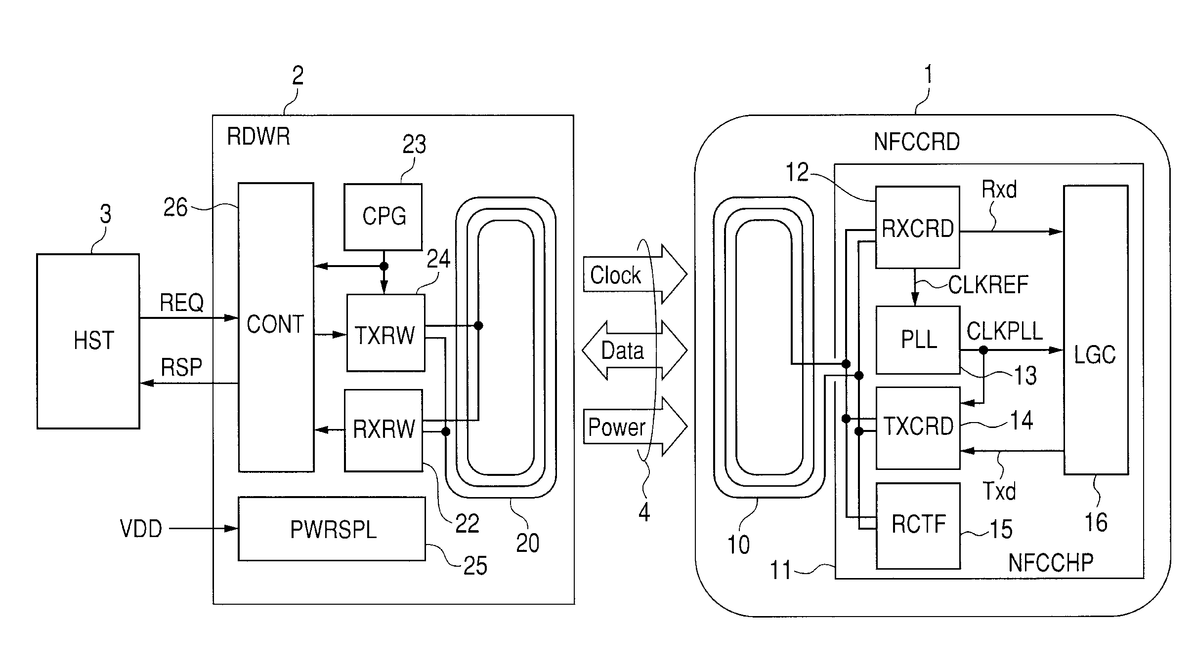
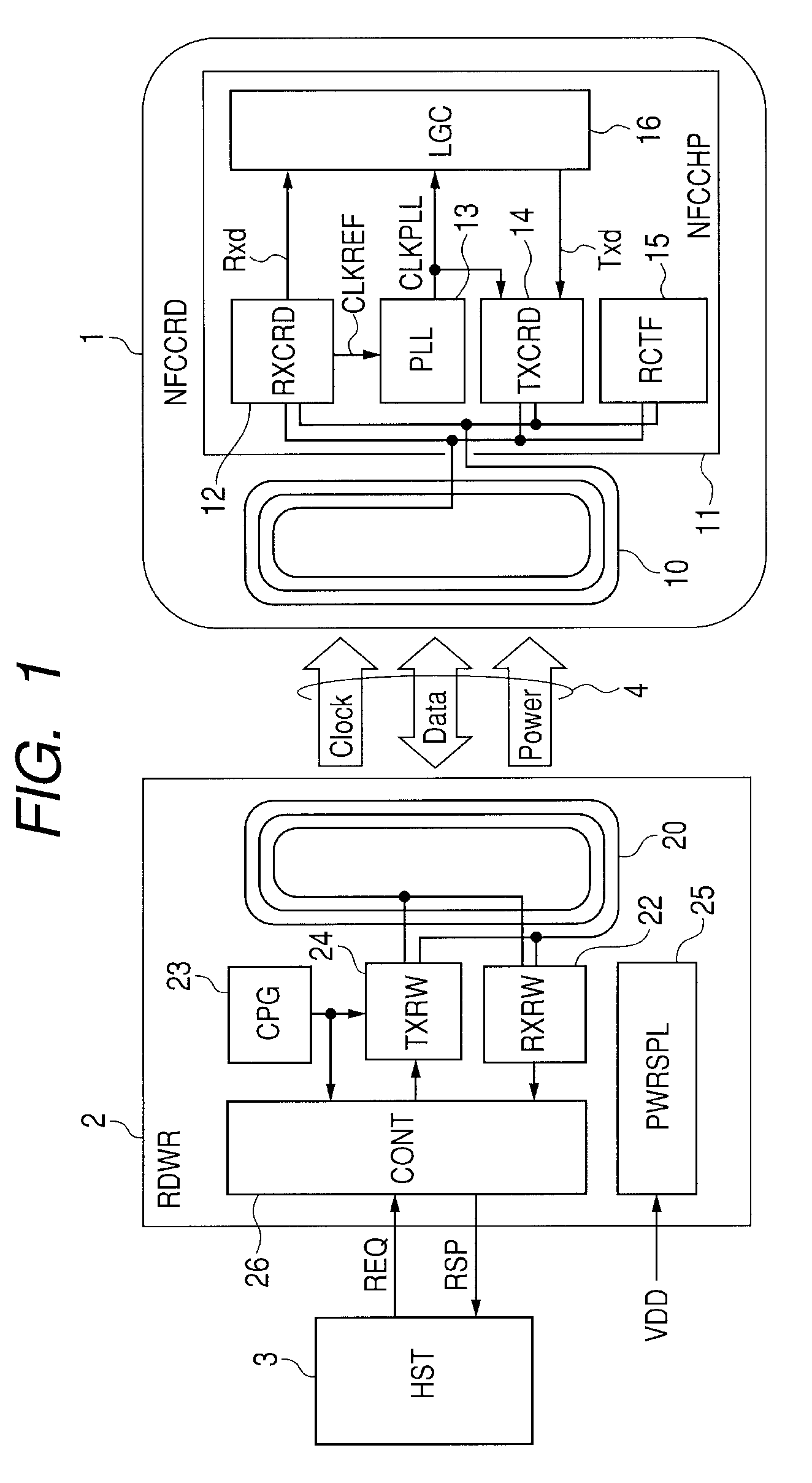
[0029]First, outline of representative embodiments of the invention disclosed in the application will be described. Reference numerals in the diagrams, referred to with parentheses in the description of the outline of the representative embodiments, just indicate components included in the concept of the components to which the reference numerals are designated.

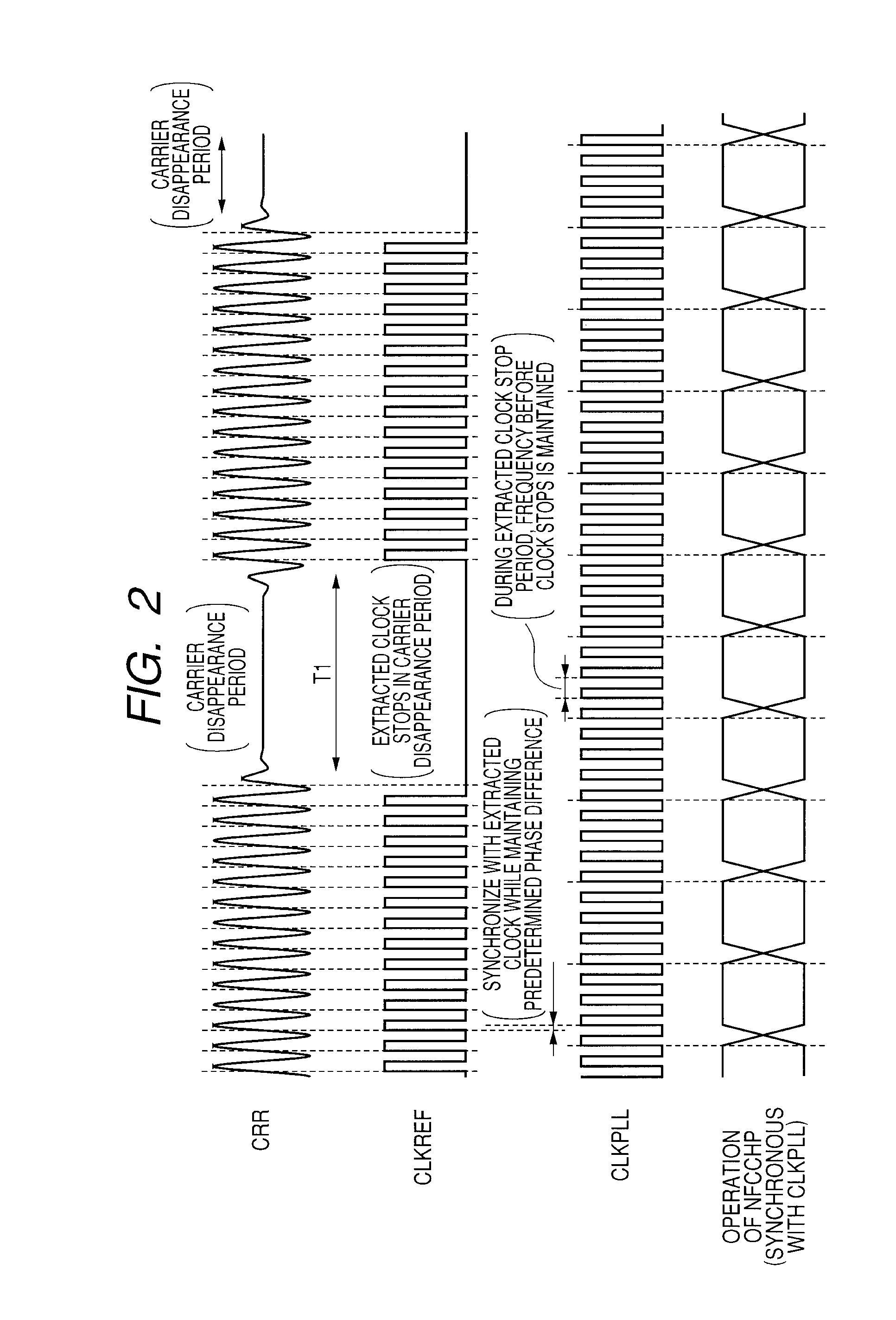
[0030][1] A semiconductor device (11, 11A) according to a representative embodiment of the present invention has: a reception circuit (12) to receive an amplitude-modulated carrier wave from an antenna (10), to demodulate it, and to extract a clock signal (CLKREF) from the carrier wave (CRR); a transmission circuit (14) to transmit a signal modulated on the basis of transmission data from the antenna; a logic circuit (16) to perform a data process for transmission / reception by the transmission circuit and the reception circuit; and a PLL circuit (13) to receive the clock signal extracted by the recept...


PUM


Abstract

The present invention provides a noncontact interface technique capable of performing communication operation without stopping an internal operation even when a clock signal cannot be extracted from a carrier wave. In a semiconductor device that receives a modulated carrier wave from an antenna, generates an internal clock signal on the basis of a clock signal extracted from the received carrier wave, and performs operation synchronously with the internal clock signal, a PLL circuit that receives the extracted clock signal and generates the internal clock signal is provided with a voltage control oscillation function. In the case where the clock signal extracted from the carrier wave is discretely interrupted, the function makes the internal clock signal maintained at a frequency immediately before the interruption. With the configuration, even when the clock signal extracted from the carrier wave is interrupted, internal data processes such as decoding and bus interfacing can be continued.

Description

CROSS-REFERENCE TO RELATED APPLICATION[0001]The disclosure of Japanese Patent Application No. 2009-19538 filed on Jan. 30, 2009 including the specification, drawings and abstract is incorporated herein by reference in its entirety.BACKGROUND OF THE INVENTION[0002]The present invention relates to a semiconductor device, a portable communication terminal, an IC card, and a microcomputer having a near field communication (NFC) function using electromagnetic induction.[0003]In a noncontact communication system, a noncontact communication card operates synchronously with a clock signal extracted from a carrier wave supplied from a reader / writer. Therefore, when the carrier wave disappears during communication, the clock signal cannot be extracted, and the operation of the communication card is stopped. For example, in the case of inputting an ASK (Amplitude Shift Keying) 100% modulation signal whose modulation target is 100% of amplitude from an antenna, the carrier wave disappears durin...

Claims


Application Information

Patent Timeline
IPC IPC(8): H04M1/00H04B1/40G06K7/10G06K19/07H03K7/02H03L7/08H03L7/093H03L7/14H04B5/02H04L7/033H04L27/04H04L27/06
CPCG06K7/10237H04L7/0025H04B1/40G06K19/0723H04L25/49H04B7/00H03L7/089H03L7/08H03L7/14
Inventor MORITA, SHINYAMAMOTO, NORIHISA
Owner RENESAS ELECTRONICS CORP
Why Eureka
Try Eureka