Organic electroluminescent device and electronic apparatus

Active Publication Date: 2010-08-12
SEIKO EPSON CORP
View PDF3 Cites 17 Cited by
  • Summary
  • Abstract
  • Description
  • Claims
  • Application Information

AI Technical Summary

Benefits of technology

[0021]With the above structure, an electronic appa

Problems solved by technology

For example, an organic EL device in the related art has a problem in that it cannot provide sufficient color reproducibility when applied to a display because light output from light-emitting layers has a wide spectral peak and low luminous intensity.
If vaporization occurs in the planarizing layer covered with the highly hermetic layers, the generated gas cannot be released and may damage the anodes and the insulating

Method used


Image

  • Organic electroluminescent device and electronic apparatus
  • Organic electroluminescent device and electronic apparatus
  • Organic electroluminescent device and electronic apparatus

Examples


first embodiment

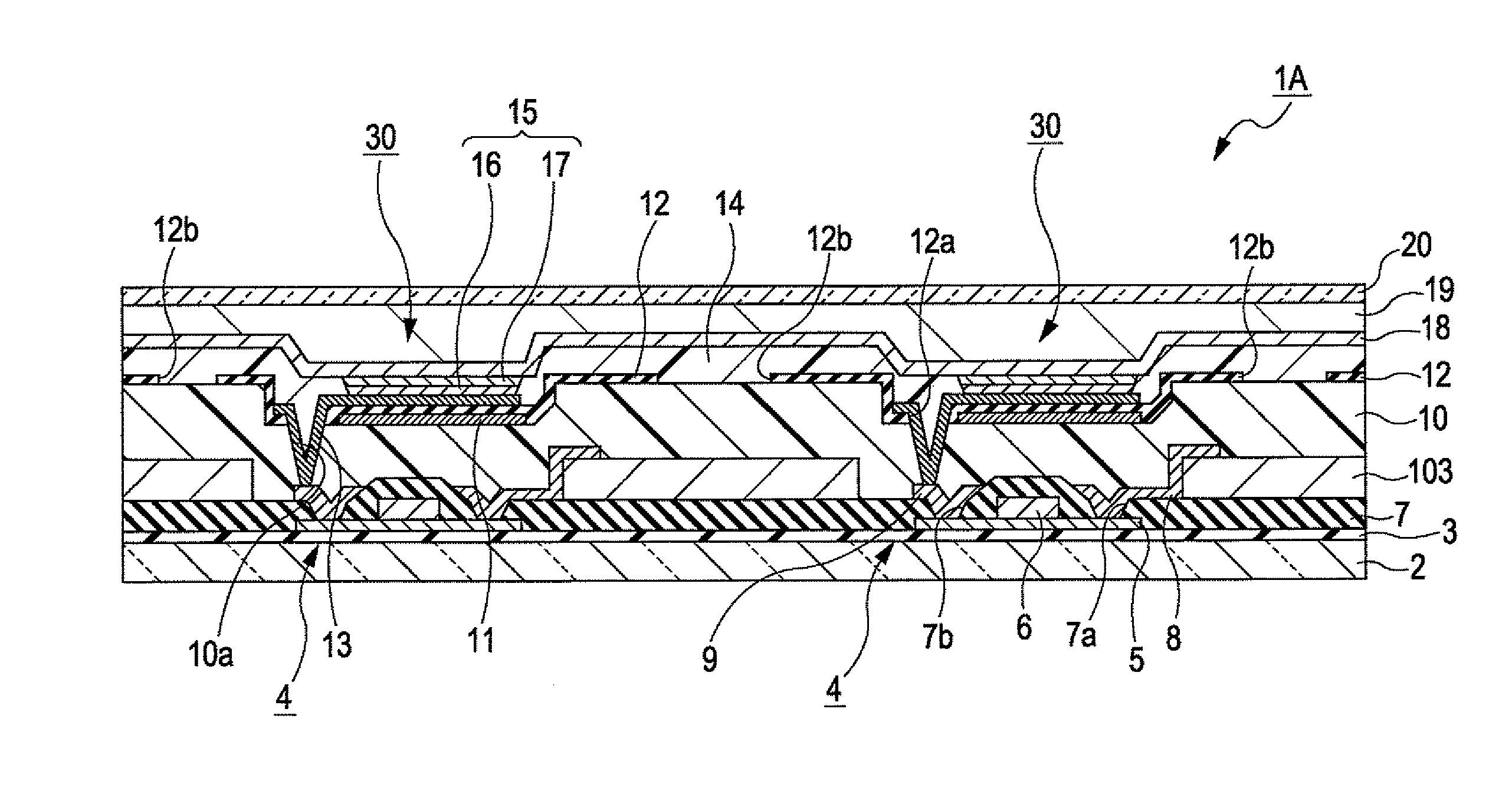
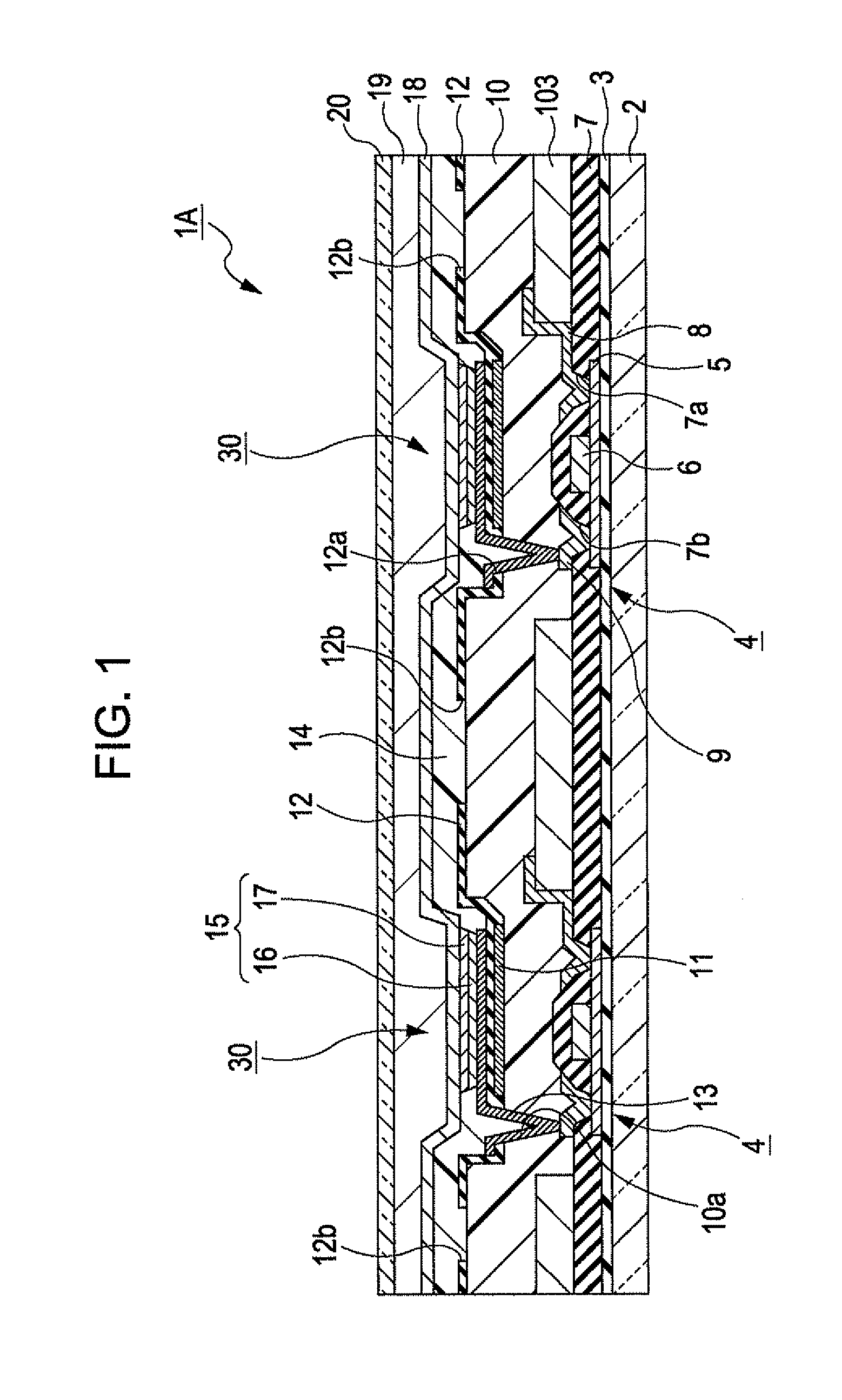
[0029]An organic EL device according to a first embodiment of the invention will now be described with reference to FIGS. 1 to 4. For clarity of the drawings, the thicknesses and sizes of individual components such as layers and parts are shown not to scale throughout all drawings so that they are large enough to be visible in the drawings.

[0030]Organic EL Device

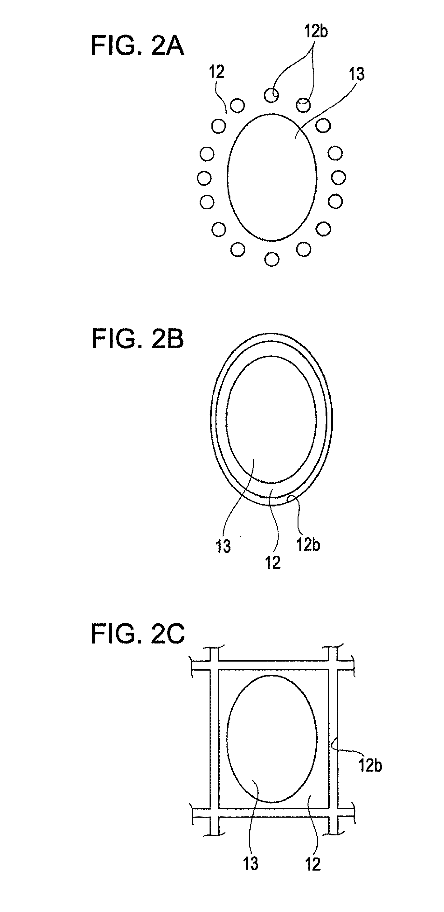
[0031]First, an organic EL device 1A according to this embodiment will be described using FIGS. 1 and 2. FIG. 1 is a sectional view schematically showing the structure of the organic EL device 1A according to this embodiment. As shown, the organic EL device 1A according to this embodiment is a top-emission organic EL device in which light emitted from functional layers 15 of numerous organic EL elements (light-emitting elements) 30 formed on a substrate 2 is output from a sealing substrate 20 disposed opposite the substrate 2 on which the organic EL elements 30 are formed.

[0032]The substrate 2 is formed of, for example, glas...

second embodiment

[0064]FIG. 5 is a diagram showing an organic EL device 1B according to a second embodiment of the invention. The organic EL device 1B according to this embodiment is partially the same as the organic EL device 1A according to the first embodiment; it differs in that the bank 14 has through-holes 14b (second through-holes). In this embodiment, therefore, the same components as those of the first embodiment are indicated by the same reference numerals, and a detailed description thereof will be omitted.

[0065]FIG. 5 is a schematic sectional view, corresponding to FIG. 4A, of the organic EL device 1B according to this embodiment. In the organic EL device 1B according to this embodiment, the bank 14 has the through-holes 14b extending through the bank 14 to reach the planarizing layer 10 via the through-holes 12b. The through-holes 14b are formed by, for example, photolithography before annealing.

[0066]In this embodiment, impurities that generate gas in the planarizing layer 10 can be re...


PUM


Abstract

An organic electroluminescent device includes a substrate; a plurality of light-emitting elements disposed on the substrate and including first transparent electrodes, a second transparent electrode, and light-emitting layers held therebetween; reflective layers disposed opposite the light-emitting layers with the first electrodes therebetween; a first insulating film disposed between the substrate and the reflective layers and formed of an organic material; and a second insulating film disposed between the first electrodes and the reflective layers so as to cover the reflective layers and the first insulating film. The second insulating film has a first through-hole at a position not overlapping the first electrodes in plan view. The first through-hole extends through the second insulating film to reach the first insulating film.

Description

BACKGROUND[0001]1. Technical Field[0002]The present invention relates to organic electroluminescent (EL) devices and electronic apparatuses.[0003]2. Related Art[0004]Organic EL devices having numerous organic EL elements on substrates are known in the related art. An organic EL device includes a planarizing layer covering components, such as thin-film transistors (TFTs) and wiring lines, formed on a substrate, electrodes (anodes) formed on the planarizing layer, a bank having openings separating the electrodes, functional layers formed in the openings of the bank, and an electrode (cathode) formed so as to cover the functional layers.[0005]Extensive research and development has been conducted on organic EL devices with the growing need for low-power, lightweight flat displays, and various production methods and various device configurations with improved display characteristics have been proposed (see, for example, the specification of Japanese Patent No. 3,328,297 and JP-A-2003-123...

Claims


Application Information

Patent Timeline
IPC IPC(8): H01L33/00
CPCH01L27/3244H01L27/3246H01L27/1248H01L51/5271H01L27/3258H10K59/122H10K59/12H10K59/124H10K50/856
Inventor TAKEI, SHUICHI
Owner SEIKO EPSON CORP
Why Eureka
Try Eureka