Unit pixel improving image sensitivity and dynamic range

a unit pixel and image sensitivity technology, applied in the field of unit pixel, can solve the problems of reducing the dynamic range and low illumination conditions of the image sensor including the pixel having those electrical characteristics, and achieve the effect of improving low illumination conditions and increasing dynamic rang

Inactive Publication Date: 2010-08-12
SILICONFILE TECH INC
View PDF5 Cites 3 Cited by
  • Summary
  • Abstract
  • Description
  • Claims
  • Application Information

AI Technical Summary

Benefits of technology

[0029]The present invention provides a unit pixel for improvi

Problems solved by technology

As described above, since the junction capacitor is changed in proportion to the voltage value dropped in the floating diffusion area FD, there is a probl

Method used


Image

  • Unit pixel improving image sensitivity and dynamic range
  • Unit pixel improving image sensitivity and dynamic range
  • Unit pixel improving image sensitivity and dynamic range

Examples


Embodiment Construction

[0042]Exemplary embodiments of the present invention will now be described in detail with reference to the accompanying drawings.

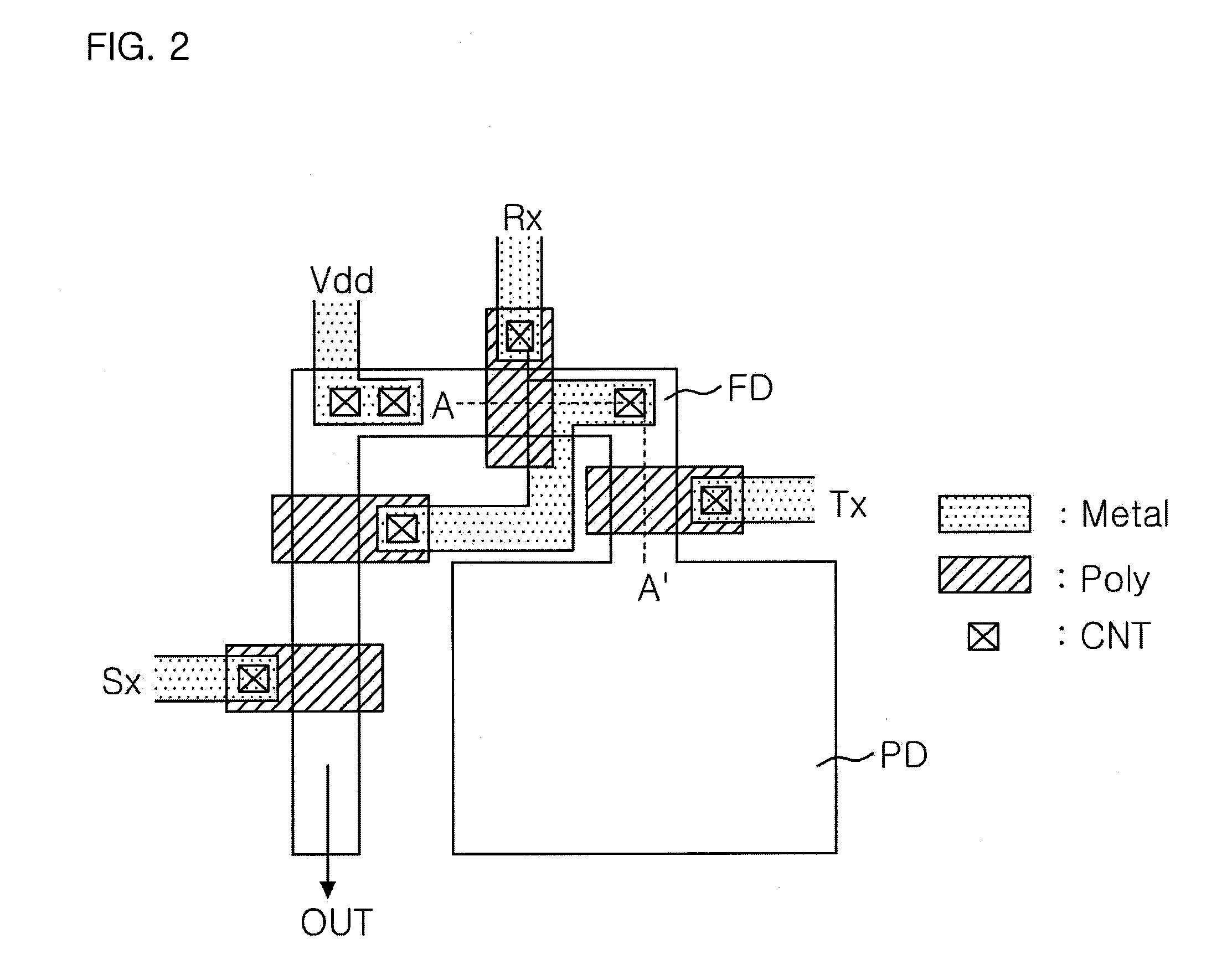
[0043]FIG. 2 illustrates a layout of a general unit pixel.

[0044]Referring to FIG. 2, gate terminals are illustrated as hatched rectangles and may be made of polycrystalline silicon.

[0045]Metal lines are illustrated as rectangles filled with dots, and the metal lines, the gate terminals, and diffusion areas are electrically connected through contacts illustrated as squares having X marks.

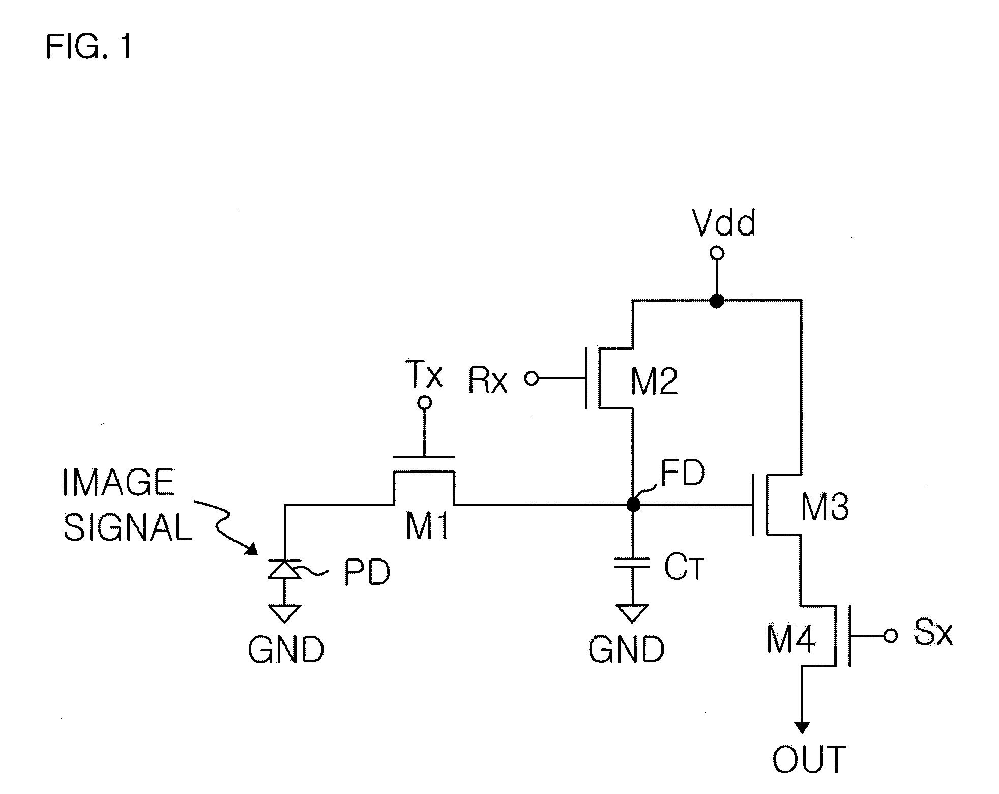
[0046]Referring to FIG. 2, the unit pixel includes a photodiode PD and an image signal conversion circuit. The image signal conversion circuit includes a transfer transistor, a reset transistor, a conversion transistor, and a selection transistor.

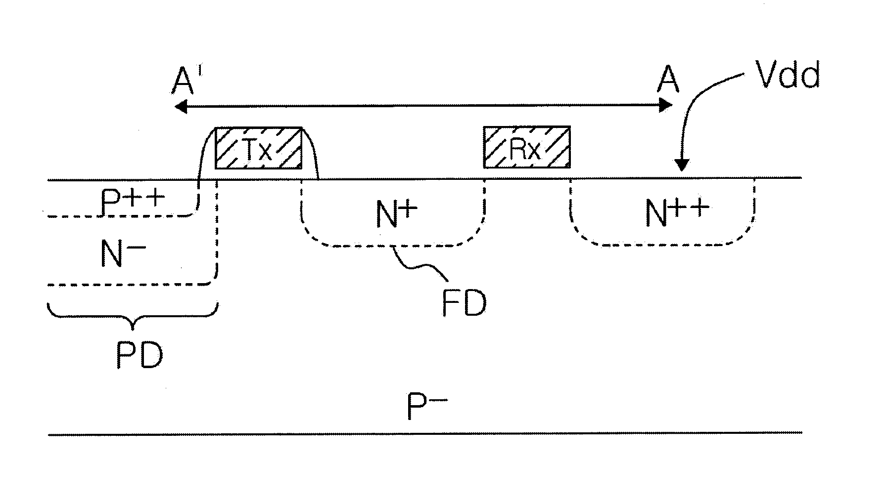
[0047]The transfer transistor includes a photodiode area PD that serves as a drain terminal and a source terminal, a floating diffusion area FD, and a gate terminal applied with a transfer control signal Tx. The reset transistor in...


PUM


Abstract

Provided are a unit pixel for improving sensitivity in low illumination conditions and a method of manufacturing the unit pixel. The unit pixel includes: a photodiode generating image charges corresponding to an image signal; a transfer transistor transferring the image charges to a floating diffusion area; and a reset transistor having a terminal connected to the floating diffusion area and the other terminal applied with a power supply, wherein concentration of impurity ions implanted into the floating diffusion area is lower than concentration of impurity ions implanted into a diffusion area of the reset transistor applied with the power supply.

Description

BACKGROUND OF THE INVENTION[0001]1. Field of the Invention[0002]The present invention relates to a unit pixel, and more particularly, to a unit pixel for improving sensitivity in low illumination conditions and increasing a dynamic range.[0003]2. Description of the Related Art[0004]FIG. 1 is a circuit diagram of a unit pixel included in an image sensor.[0005]Referring to FIG. 1, the unit pixel includes a photodiode PD and an image signal conversion circuit. The image signal conversion signal includes a transfer transistor M1, a reset transistor M2, a conversion transistor M3, and a selection transistor M4.[0006]The photodiode PD generates image charges corresponding to an image signal. The image charges are transferred to a floating diffusion area FD through the transfer transistor M1 that is switched on or off in response to a transfer control signal Tx.[0007]The reset transistor M2 resets the floating diffusion area FD[0008]The conversion transistor M3 generates a conversion volta...

Claims


Application Information

Patent Timeline
IPC IPC(8): H01L27/146H01L31/18
CPCH01L27/14601H01L27/14689H01L27/14643H01L27/146
Inventor LEE, DO-YOUNG
Owner SILICONFILE TECH INC
Why Eureka
Try Eureka