Nonvolatile memory device and method of writing data to nonvolatile memory device

a nonvolatile memory and data technology, applied in the direction of information storage, static storage, digital storage, etc., can solve the problems of difficult miniaturization of flash memory, limited speed, and difficult to reduce the size of flash memory, so as to prolong the life of the device and improve the reliability of the operation of the nonvolatile memory device.

Active Publication Date: 2010-08-12
PANASONIC SEMICON SOLUTIONS CO LTD
View PDF7 Cites 21 Cited by
  • Summary
  • Abstract
  • Description
  • Claims
  • Application Information

AI Technical Summary

Benefits of technology

[0034]The present invention has the above described configuration, and achieves the advantages described below. That is, reliability of the operation of the nonvolatile memory device can be improved and the life of the device can be extended, in a nonvolatile memory device including a memory cell array including plural resistance variable elements which are switchable between plural resistance states in response to electric pulses with the same polarity.

Problems solved by technology

It has been pointed out that since the flash memory has a structure for accumulating electric charges on the floating gate in a high electric field, there is a limitation on reduction of the size, and it is difficult to miniaturize the flash memory, which is required to achieve a larger capacity.
Because of such a property, the flash memory requires a very long time for rewriting and has a limitation on an increase in the speed.
In this case, the element would switch back from the low-resistance state to the high-resistance state unexpectedly (incorrect operation), or would be broken down due to an excess current.

Method used


Image

  • Nonvolatile memory device and method of writing data to nonvolatile memory device
  • Nonvolatile memory device and method of writing data to nonvolatile memory device
  • Nonvolatile memory device and method of writing data to nonvolatile memory device

Examples


embodiment 1

Configuration

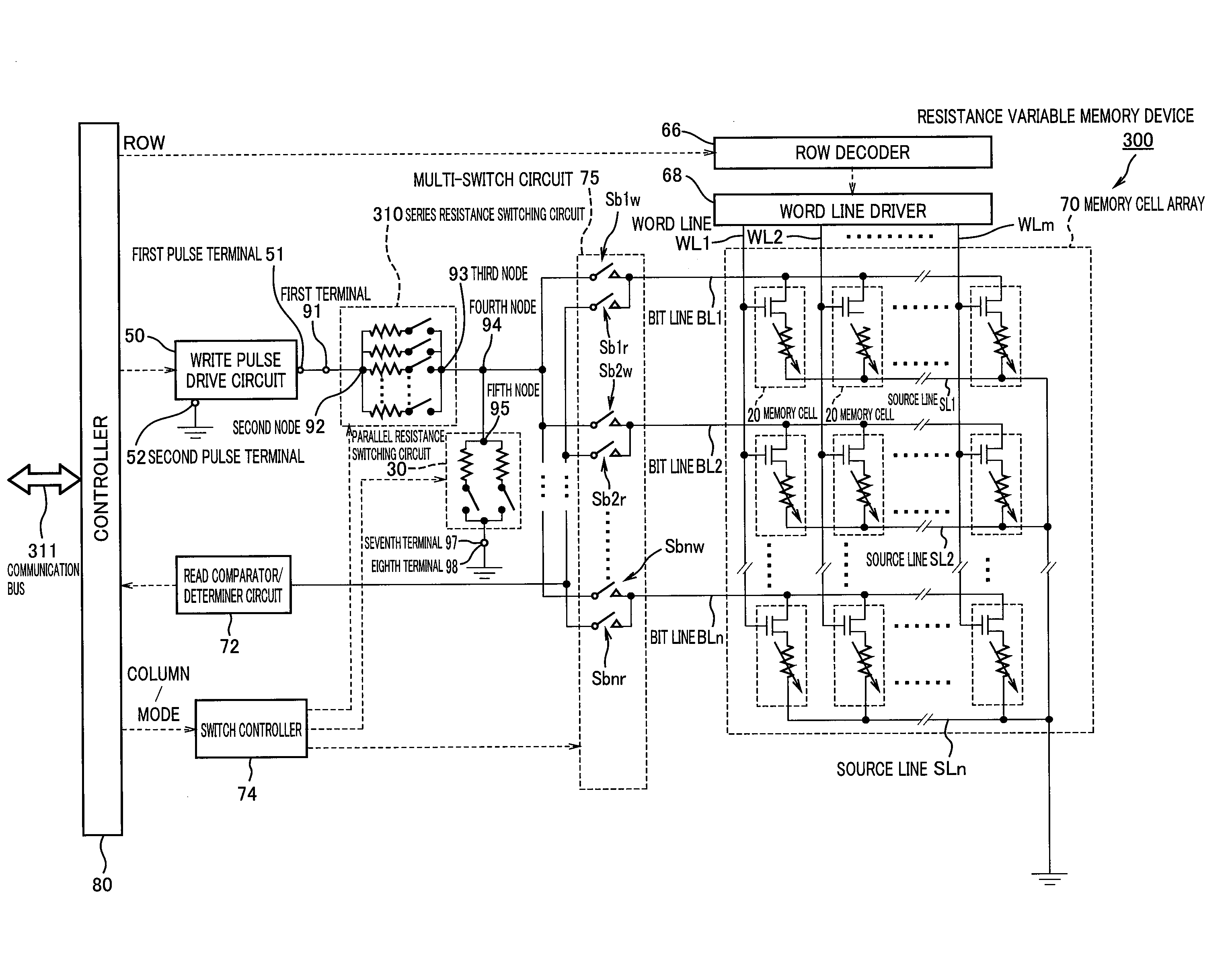
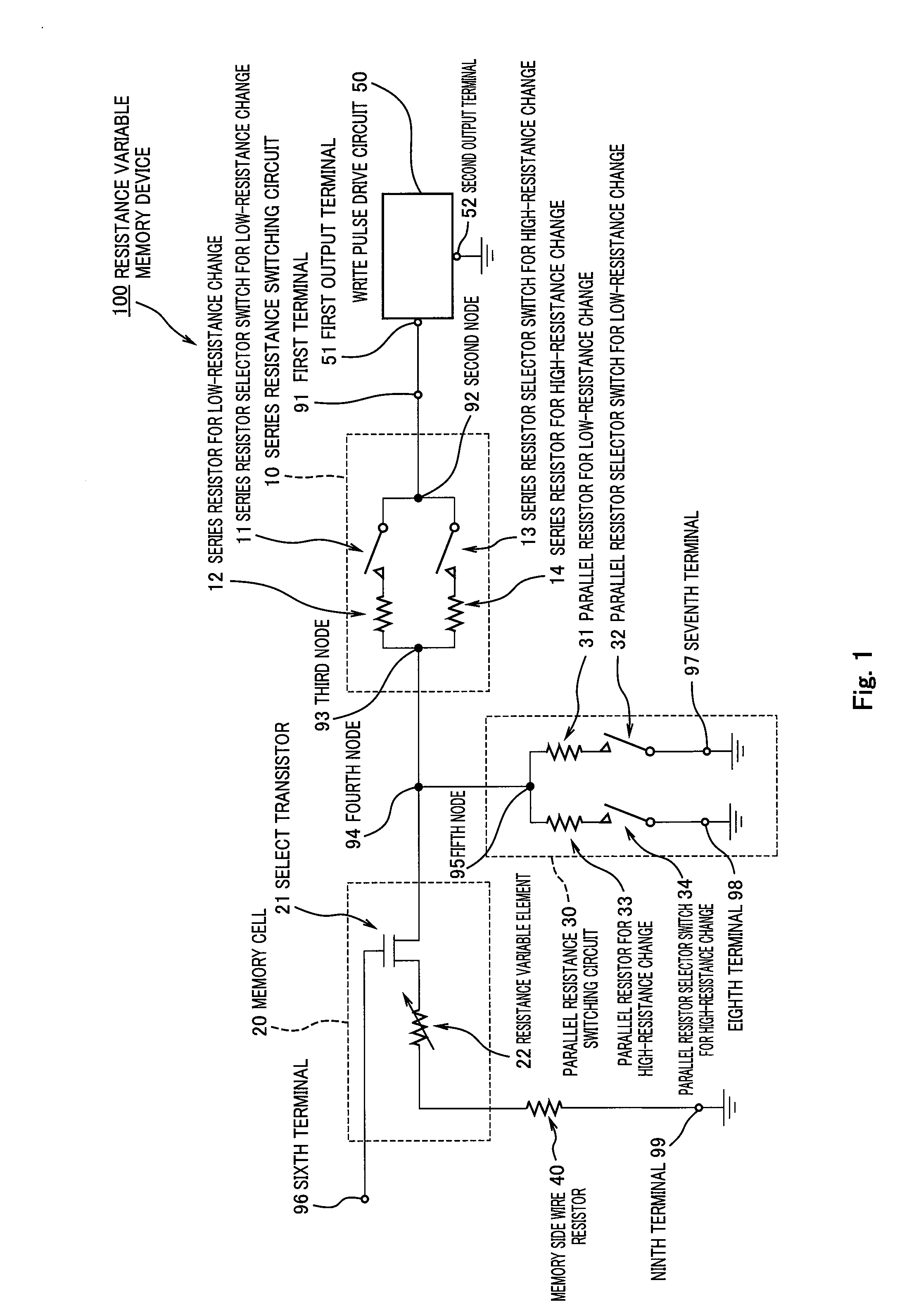
[0199]FIG. 5 is a block diagram showing an exemplary nonvolatile memory device according to Embodiment 1 of the present invention. With reference to FIG. 5, a nonvolatile memory device 300 of this embodiment will be described. The constituents which are identical to those of Configuration 1 (FIG. 1) and Configuration 2 (FIG. 5) are identified by the same reference numbers and names and will not be described repetitively.

[0200]As shown in FIG. 5, the nonvolatile memory device 300 comprises as major constituents, a memory cell array 70, a row decoder 66, a word line driver 68 (second select circuit), a multi-switch circuit 75 (first select circuit), a series resistance switching circuit 310, a parallel resistance switching circuit 30, a write pulse drive circuit 50, a read comparator / determiner circuit 72, a switch controller 74, a controller 80, and a communication bus 311.

[0201]The memory cell array 70 includes plural memory cells 20. In the memory cell array 70, the me...

embodiment 2

Configuration

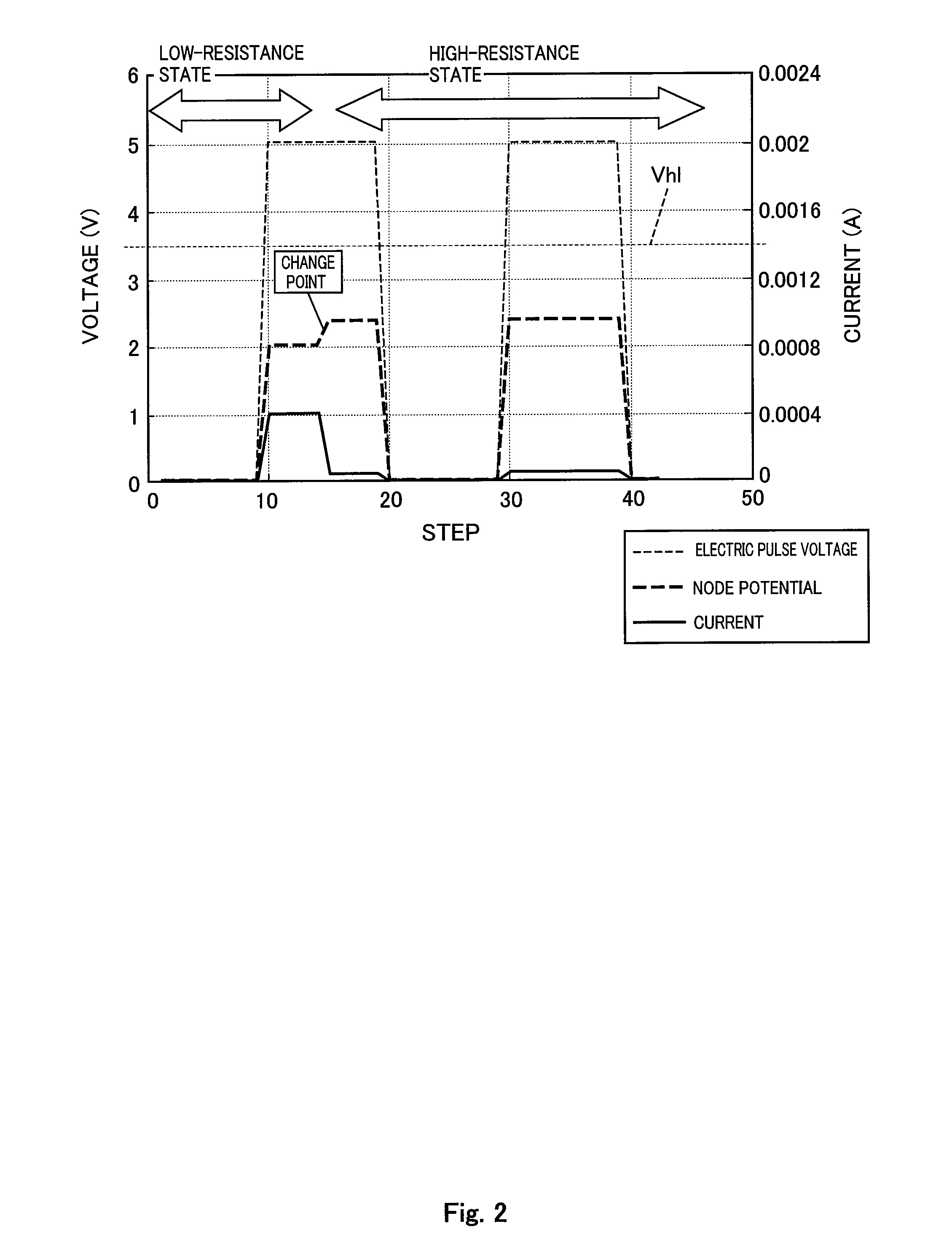
[0257]In Embodiment 1, as shown in FIG. 6, the device is configured assuming that the distribution of Vlh and the distribution of Vhl do not overlap with each other. However, the two distributions may sometimes overlap with each other. If the distributions overlap with each other, proper control would be difficult in the configuration of Embodiment 1. FIG. 10 is a conceptual diagram showing a distribution of a high-resistance state attaining voltage and a distribution of a low-resistance state attaining voltage of resistance variable elements in the memory cell array in a case where there are significant variations in the these voltages. In the example shown in FIG. 10 in which there are significant variations, there is a tendency that an incorrect operation occurs, in which the resistance variable element which has switched to the high-resistance state switches back to the low-resistance state or the resistance variable element which has switched to the low-resistance ...


PUM


Abstract

A nonvolatile memory device (300) is provided, including a memory cell array having plural resistance variable elements which are switchable between plural resistance states in response to electric pulses with the same polarity. A series resistance setting unit (310) is provided between the memory cell array (70) and an electric pulse application unit (50). The series resistance setting unit is controlled to change a resistance value of a series current path with a predetermined range with time in at least one of a case where the selected resistance variable element is switched from a low-resistance state to a high-resistance state and a case where the selected resistance variable element is switched from the high-resistance state to the low-resistance state.

Description

TECHNICAL FIELD[0001]The present invention relates to a nonvolatile memory device and a method of writing data to the nonvolatile memory device. More particularly, the present invention relates to a nonvolatile memory device configured to write data to resistance variable elements utilizing a difference in a voltage level of electric pulses with the same polarity, and a method of writing data to the nonvolatile memory device.BACKGROUND ART[0002]Nonvolatile memory devices are commonly mounted in portable apparatus such as cellular phones or digital cameras and the use of them has been spreading at a rapid pace. In recent years, in many occasions, audio data and image data are used. Accordingly, there has been a strong demand for nonvolatile memory devices which have larger capacities and are operable at higher speeds. Furthermore, in fields of nonvolatile memory devices for use with portable apparatus, a demand for lower electric power consumption has been increasing.[0003]At present...

Claims


Application Information

Patent Timeline
Patent Type & Authority Applications(United States)
IPC IPC(8): G11C11/00G11C7/22
CPCG11C13/00G11C13/0038G11C2213/79G11C2013/0078G11C2213/15G11C13/0069
Inventor KATOH, YOSHIKAZUSHIMAKAWA, KAZUHIKO
Owner PANASONIC SEMICON SOLUTIONS CO LTD
Why Eureka
Try Eureka